- 快召唤伙伴们来围观吧
- 微博 QQ QQ空间 贴吧
- 文档嵌入链接
- 复制
- 微信扫一扫分享
- 已成功复制到剪贴板
时序逻辑
展开查看详情
1 .Chapter 3 Digital Logic Structures
2 .3- 2 Combinational vs. Sequential Combinational Circuit always gives the same output for a given set of inputs ex: adder always generates sum and carry, regardless of previous inputs Sequential Circuit stores information output depends on stored information (state) plus input so a given input might produce different outputs, depending on the stored information example: ticket counter advances when you push the button output depends on previous state useful for building “memory” elements and “state machines”
3 .3 To retain their state values, sequential circuits rely on feedback. Feedback in digital circuits occurs when an output is looped back to the input. A simple example of this concept is shown below. If Q is 0 it will always be 0, if it is 1, it will always be 1. Why? Sequential Circuits
4 .A Bistable Feedback Circuit Consider the two possible cases: Q = 0: then Q = 1 and Q = 0 (consistent) Q = 1: then Q = 0 and Q = 1 (consistent) Bistable circuit stores 1 bit of state in the state variable, Q (or Q ) But there are no inputs to control the state
5 .3- 5 R-S Latch: Simple Storage Element R is used to “reset” or “clear” the element – set it to zero. S is used to “set” the element – set it to one. If both R and S are one, out could be either zero or one. “quiescent” state -- holds its previous value note: if a is 1, b is 0, and vice versa 1 0 1 1 1 1 0 0 1 1 0 0 1 1
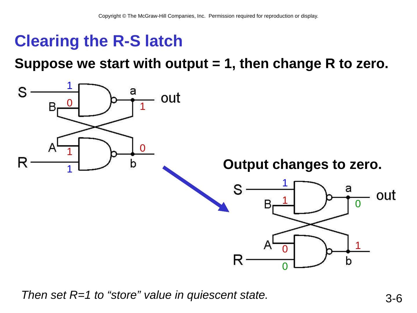
6 .3- 6 Clearing the R-S latch Suppose we start with output = 1, then change R to zero. Output changes to zero. Then set R=1 to “store” value in quiescent state. 1 0 1 1 1 1 0 0 1 0 1 0 0 0 1 1
7 .3- 7 Setting the R-S Latch Suppose we start with output = 0, then change S to zero. Output changes to one. Then set S=1 to “store” value in quiescent state. 1 1 0 0 1 1 0 1 1 1 0 0
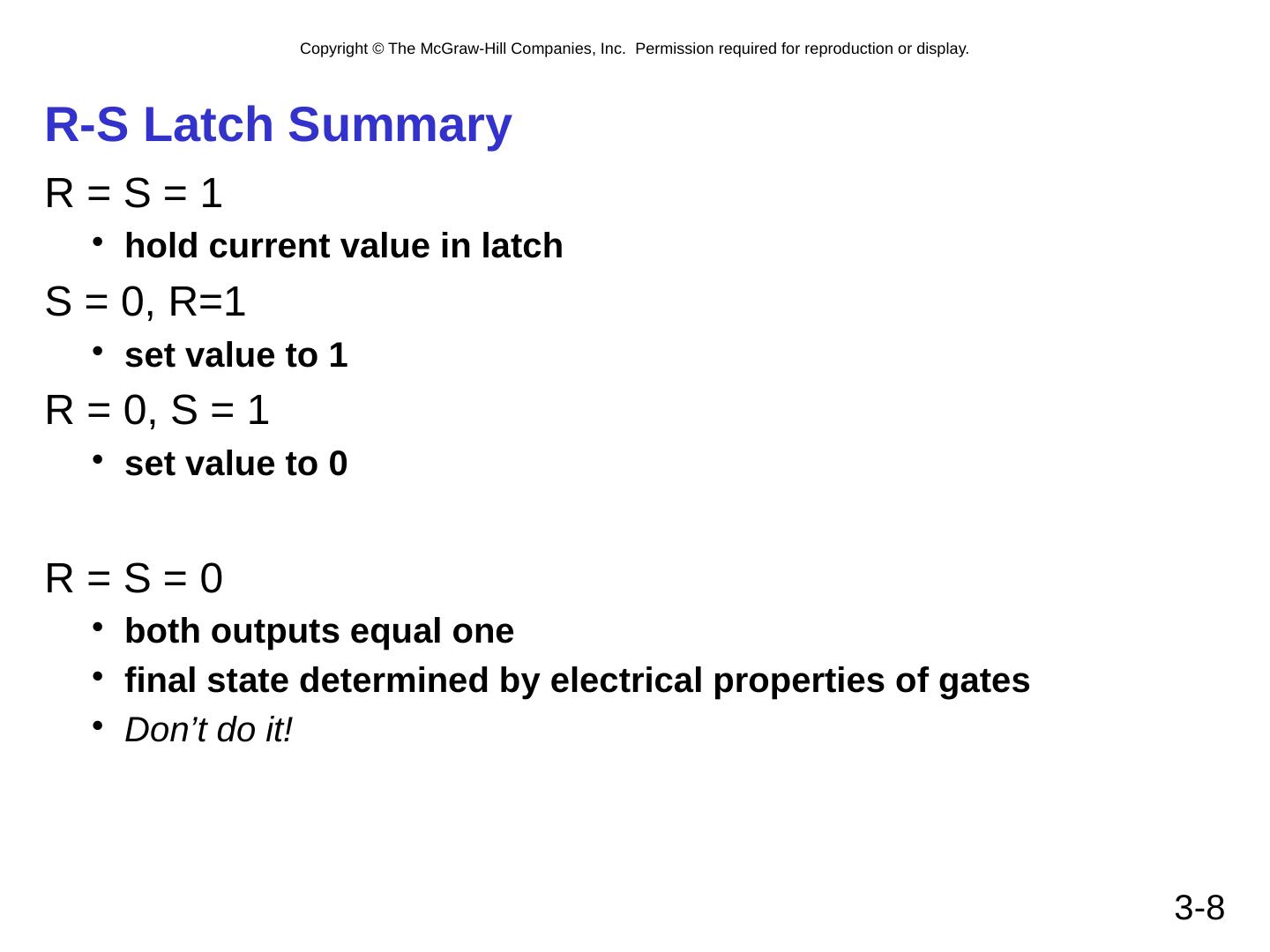
8 .3- 8 R-S Latch Summary R = S = 1 hold current value in latch S = 0, R=1 set value to 1 R = 0, S = 1 set value to 0 R = S = 0 both outputs equal one final state determined by electrical properties of gates Don’t do it!
9 .3- 9 Gated D-Latch Two inputs: D (data) and WE (write enable) when WE = 1 , latch is set to value of D S = NOT(D), R = D when WE = 0 , latch holds previous value S = R = 1
10 .3- 10 Register A register stores a multi-bit value. We use a collection of D-latches, all controlled by a common WE. When WE=1, n-bit value D is written to register.
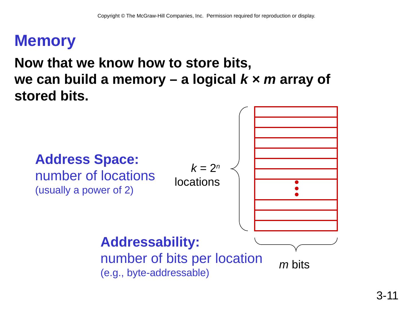
11 .3- 11 Memory Now that we know how to store bits, we can build a memory – a logical k × m array of stored bits. • • • k = 2 n locations m bits Address Space: number of locations (usually a power of 2) Addressability: number of bits per location (e.g., byte-addressable)
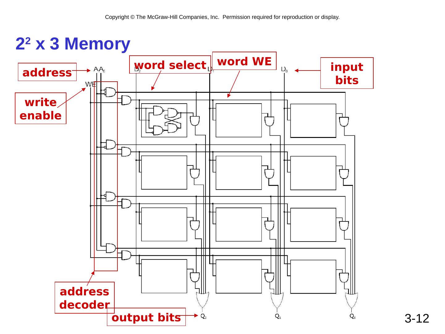
12 .3- 12 2 2 x 3 Memory address decoder word select word WE address write enable input bits output bits
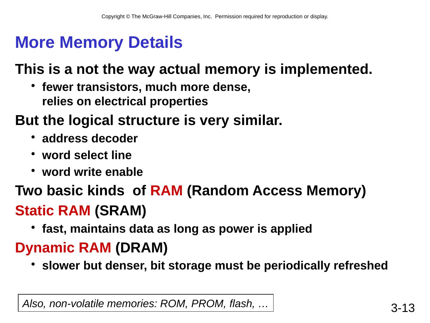
13 .3- 13 More Memory Details This is a not the way actual memory is implemented. fewer transistors, much more dense, relies on electrical properties But the logical structure is very similar. address decoder word select line word write enable Two basic kinds of RAM (Random Access Memory) Static RAM (SRAM) fast, maintains data as long as power is applied Dynamic RAM (DRAM) slower but denser, bit storage must be periodically refreshed Also, non-volatile memories: ROM, PROM, flash, …


