


- 快召唤伙伴们来围观吧
- 微博 QQ QQ空间 贴吧
- 文档嵌入链接
- 复制
- 微信扫一扫分享
- 已成功复制到剪贴板
内存层次结构:缓存系统
本文主要介绍了内存层次结构中的缓存系统。首先学习了高速缓存动力图解,存储器系统的扩展视图和内存层次结构的层次。根据以上局部性原则学习内存层次结构的操作原理和如何将地址映射到多字缓存块。举例讨论了集合关联缓存的缺点,引出缓存系统综述。
展开查看详情
1 . ECE4680 Computer Organization and Architecture Memory Hierarchy: Cache System ECE4680 Cache.1 2002-4-17 The Motivation for Caches Memory System Processor Cache DRAM °Motivation: • Large memories (DRAM) are slow • Small memories (SRAM) are fast °Make the average access time small by: • Servicing most accesses from a small, fast memory. °Reduce the bandwidth required of the large memory ECE4680 Cache.2 2002-4-17
2 . An Expanded View of the Memory System Processor Control Memory Memory Memory Memory Datapath Memory Speed: Fastest Slowest Size: Smallest Biggest Cost: Highest Lowest ECE4680 Cache.3 2002-4-17 Levels of the Memory Hierarchy Capacity Upper Level Access Time Staging Cost Xfer Unit faster CPU Registers 100s Bytes Registers <10s ns Instr. Operands prog./compiler 1-8 bytes Cache K Bytes 10-100 ns Cache $.01-.001/bit cache cntl Blocks 8-128 bytes Main Memory M Bytes Memory 100ns-1us $.01-.001 OS Pages 512-4K bytes Disk G Bytes ms Disk -3 -4 10 - 10 cents user/operator Files Mbytes Tape Larger infinite sec-min Tape Lower Level 10 -6 ECE4680 Cache.4 2002-4-17
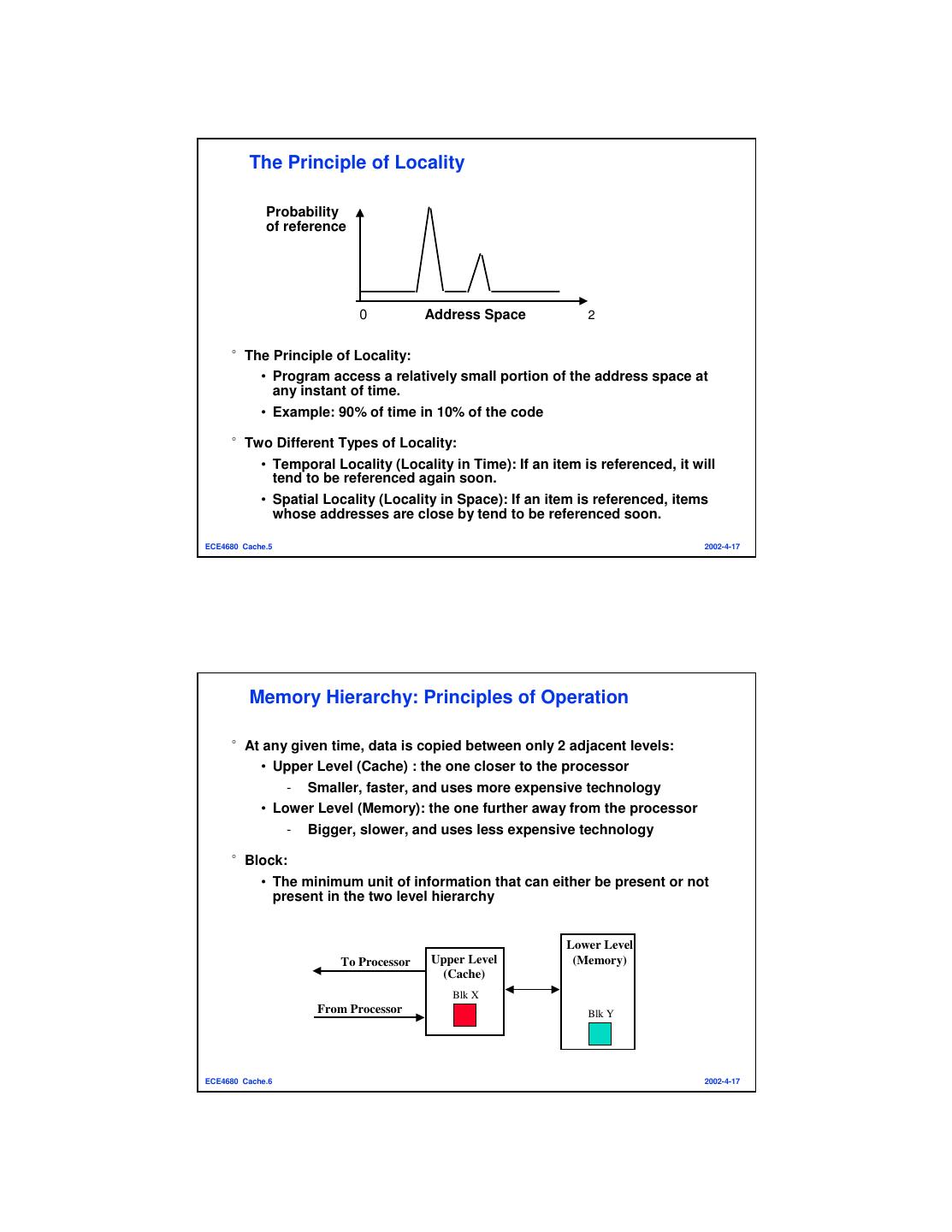
3 . The Principle of Locality Probability of reference 0 Address Space 2 °The Principle of Locality: • Program access a relatively small portion of the address space at any instant of time. • Example: 90% of time in 10% of the code °Two Different Types of Locality: • Temporal Locality (Locality in Time): If an item is referenced, it will tend to be referenced again soon. • Spatial Locality (Locality in Space): If an item is referenced, items whose addresses are close by tend to be referenced soon. ECE4680 Cache.5 2002-4-17 Memory Hierarchy: Principles of Operation °At any given time, data is copied between only 2 adjacent levels: • Upper Level (Cache) : the one closer to the processor - Smaller, faster, and uses more expensive technology • Lower Level (Memory): the one further away from the processor - Bigger, slower, and uses less expensive technology °Block: • The minimum unit of information that can either be present or not present in the two level hierarchy Lower Level To Processor Upper Level (Memory) (Cache) Blk X From Processor Blk Y ECE4680 Cache.6 2002-4-17
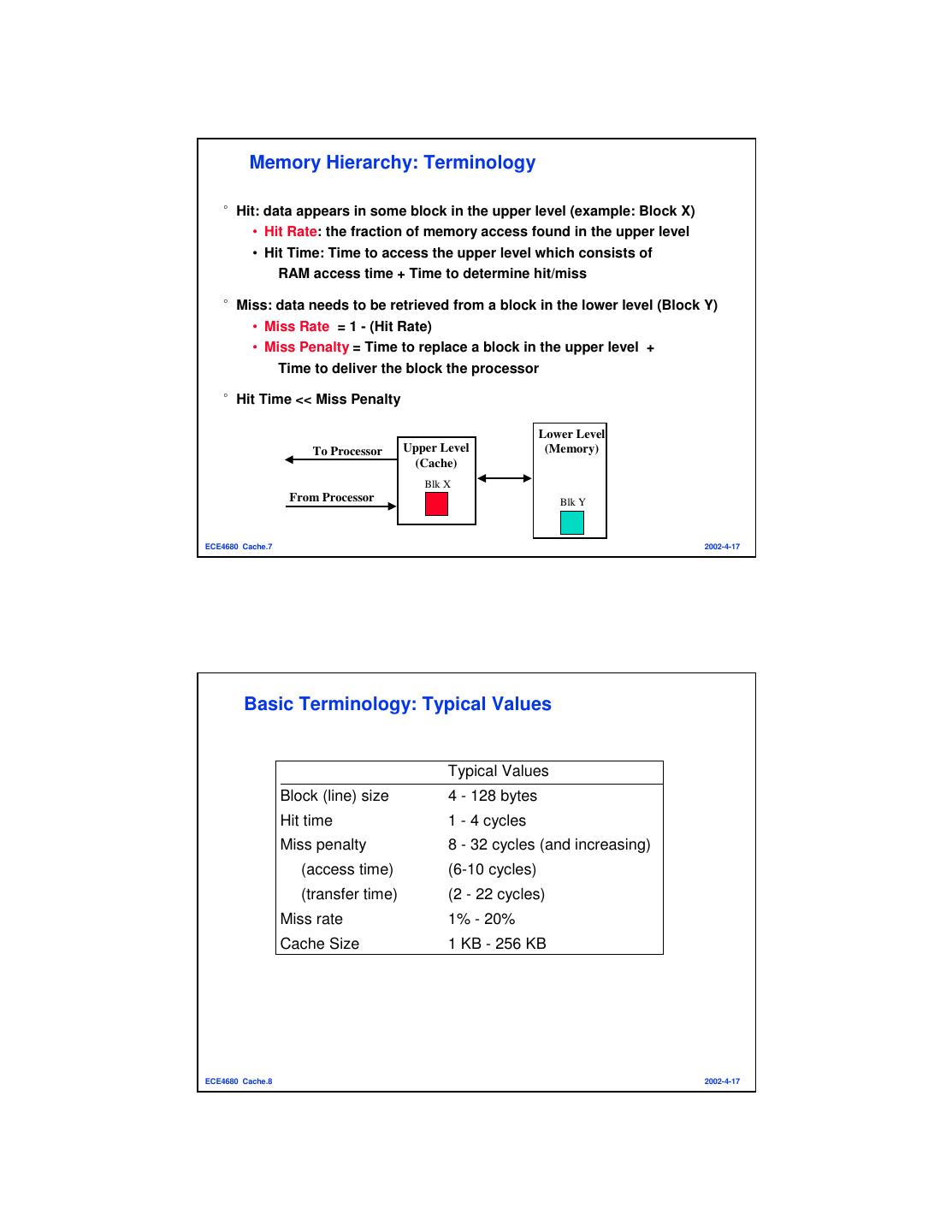
4 . Memory Hierarchy: Terminology °Hit: data appears in some block in the upper level (example: Block X) • Hit Rate: the fraction of memory access found in the upper level • Hit Time: Time to access the upper level which consists of RAM access time + Time to determine hit/miss °Miss: data needs to be retrieved from a block in the lower level (Block Y) • Miss Rate = 1 - (Hit Rate) • Miss Penalty = Time to replace a block in the upper level + Time to deliver the block the processor °Hit Time << Miss Penalty Lower Level To Processor Upper Level (Memory) (Cache) Blk X From Processor Blk Y ECE4680 Cache.7 2002-4-17 Basic Terminology: Typical Values Typical Values Block (line) size 4 - 128 bytes Hit time 1 - 4 cycles Miss penalty 8 - 32 cycles (and increasing) (access time) (6-10 cycles) (transfer time) (2 - 22 cycles) Miss rate 1% - 20% Cache Size 1 KB - 256 KB ECE4680 Cache.8 2002-4-17
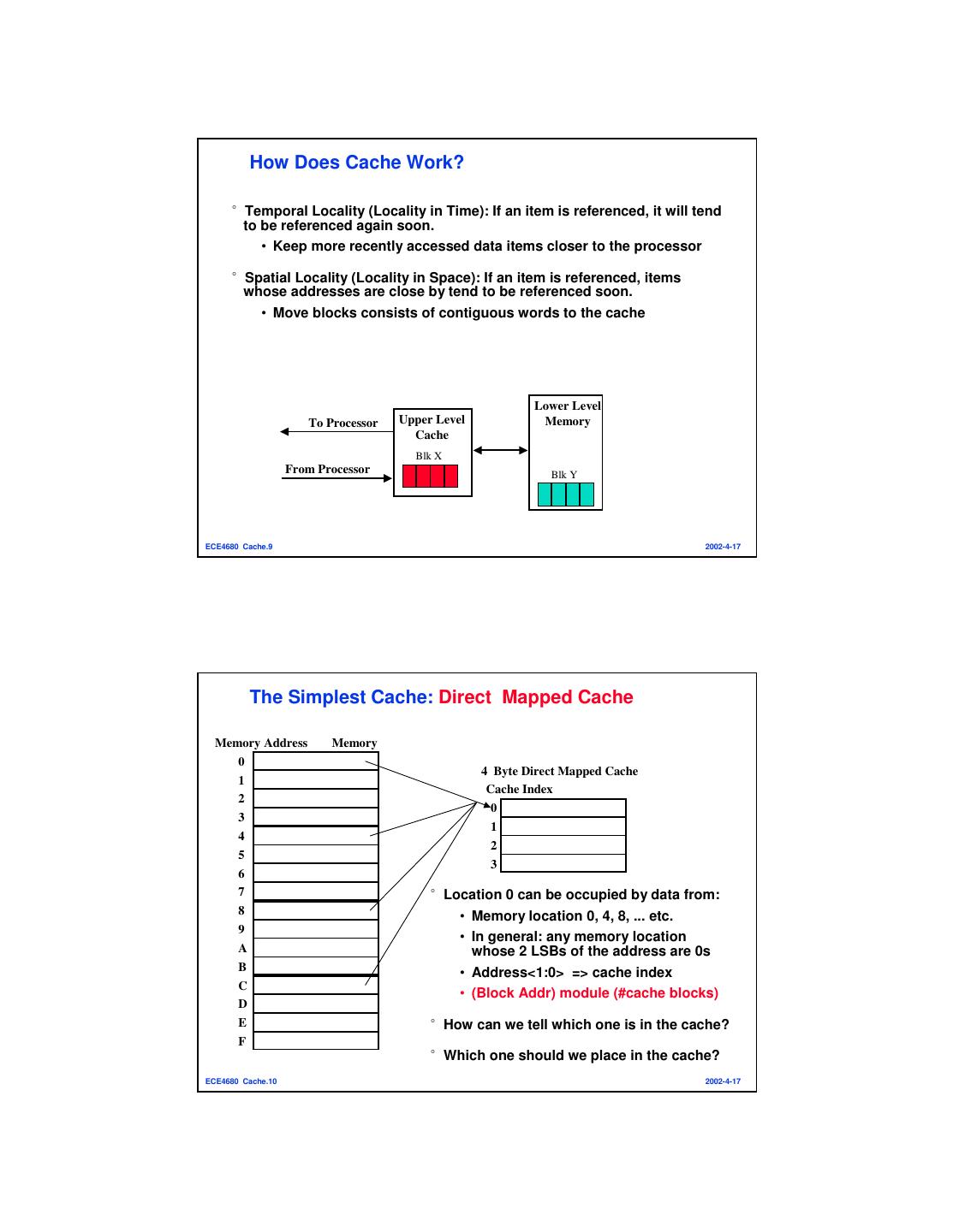
5 . How Does Cache Work? °Temporal Locality (Locality in Time): If an item is referenced, it will tend to be referenced again soon. • Keep more recently accessed data items closer to the processor °Spatial Locality (Locality in Space): If an item is referenced, items whose addresses are close by tend to be referenced soon. • Move blocks consists of contiguous words to the cache Lower Level To Processor Upper Level Memory Cache Blk X From Processor Blk Y ECE4680 Cache.9 2002-4-17 The Simplest Cache: Direct Mapped Cache Memory Address Memory 0 4 Byte Direct Mapped Cache 1 Cache Index 2 0 3 1 4 2 5 3 6 7 °Location 0 can be occupied by data from: 8 • Memory location 0, 4, 8, ... etc. 9 • In general: any memory location A whose 2 LSBs of the address are 0s B • Address<1:0> => cache index C • (Block Addr) module (#cache blocks) D E °How can we tell which one is in the cache? F °Which one should we place in the cache? ECE4680 Cache.10 2002-4-17
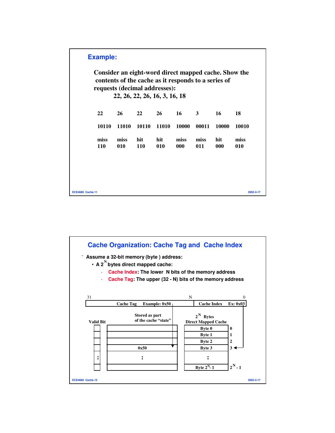
6 . Example: Consider an eight-word direct mapped cache. Show the contents of the cache as it responds to a series of requests (decimal addresses): 22, 26, 22, 26, 16, 3, 16, 18 22 26 22 26 16 3 16 18 10110 11010 10110 11010 10000 00011 10000 10010 miss miss hit hit miss miss hit miss 110 010 110 010 000 011 000 010 ECE4680 Cache.11 2002-4-17 Cache Organization: Cache Tag and Cache Index °Assume a 32-bit memory (byte ) address: N • A 2 bytes direct mapped cache: - Cache Index: The lower N bits of the memory address - Cache Tag: The upper (32 - N) bits of the memory address 31 N 0 Cache Tag Example: 0x50 Cache Index Ex: 0x03 Stored as part N 2 Bytes Valid Bit of the cache “state” Direct Mapped Cache Byte 0 0 Byte 1 1 Byte 2 2 0x50 Byte 3 3 : : : N Byte 2 N- 1 2 -1 ECE4680 Cache.12 2002-4-17
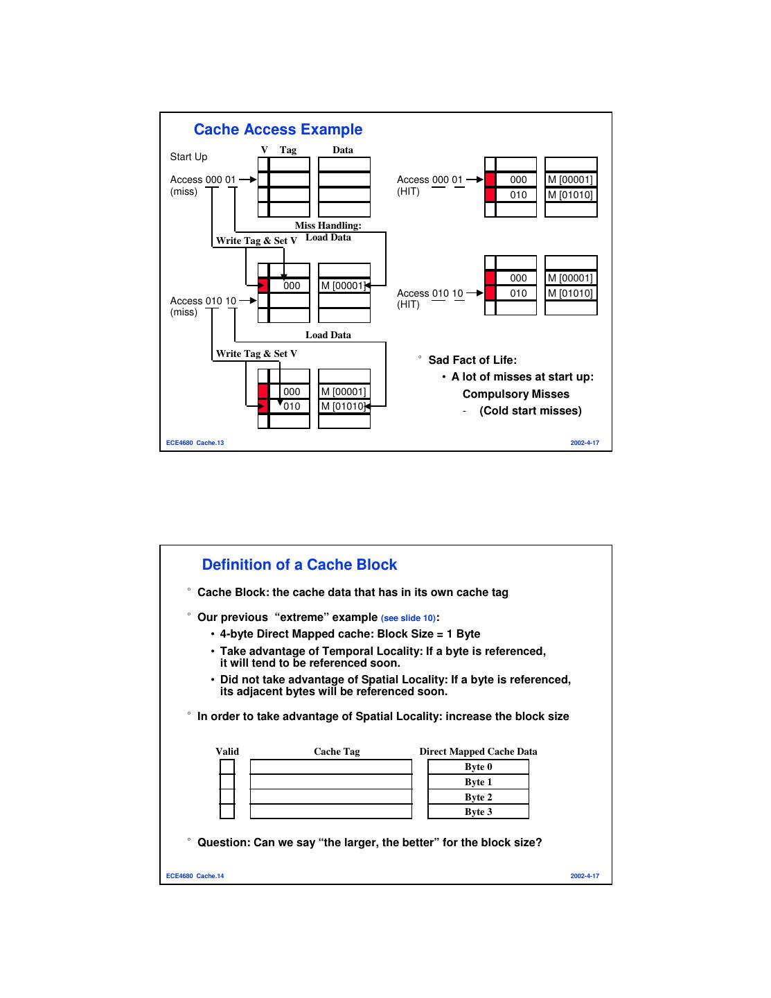
7 . Cache Access Example V Tag Data Start Up Access 000 01 Access 000 01 000 M [00001] (miss) (HIT) 010 M [01010] Miss Handling: Write Tag & Set V Load Data 000 M [00001] 000 M [00001] Access 010 10 010 M [01010] Access 010 10 (HIT) (miss) Load Data Write Tag & Set V °Sad Fact of Life: • A lot of misses at start up: 000 M [00001] Compulsory Misses 010 M [01010] - (Cold start misses) ECE4680 Cache.13 2002-4-17 Definition of a Cache Block °Cache Block: the cache data that has in its own cache tag °Our previous “extreme” example (see slide 10): • 4-byte Direct Mapped cache: Block Size = 1 Byte • Take advantage of Temporal Locality: If a byte is referenced, it will tend to be referenced soon. • Did not take advantage of Spatial Locality: If a byte is referenced, its adjacent bytes will be referenced soon. °In order to take advantage of Spatial Locality: increase the block size Valid Cache Tag Direct Mapped Cache Data Byte 0 Byte 1 Byte 2 Byte 3 °Question: Can we say “the larger, the better” for the block size? ECE4680 Cache.14 2002-4-17
8 . Example: 1 KB Direct Mapped Cache with 32 B Blocks °For a 2 ** N byte cache: • The uppermost (32 - N) bits are always the Cache Tag • The lowest M bits are the Byte Select (Block Size = 2 ** M) 31 9 4 0 Cache Tag Example: 0x50 Cache Index Byte Select Ex: 0x01 Ex: 0x00 Stored as part of the cache “state” Valid Bit Cache Tag Cache Data : : Byte 31 Byte 1 Byte 0 0 0x50 Byte 63 Byte 33 Byte 32 1 2 3 : : : : Byte 1023 Byte 992 31 ECE4680 Cache.15 2002-4-17 Mapping an Address to a Multiword Cache Block Consider a cache with 64 Blocks and a block size of 16 bytes. What block number does byte address 1200 map to? [1200/16] module 64 = 11 ECE4680 Cache.16 2002-4-17
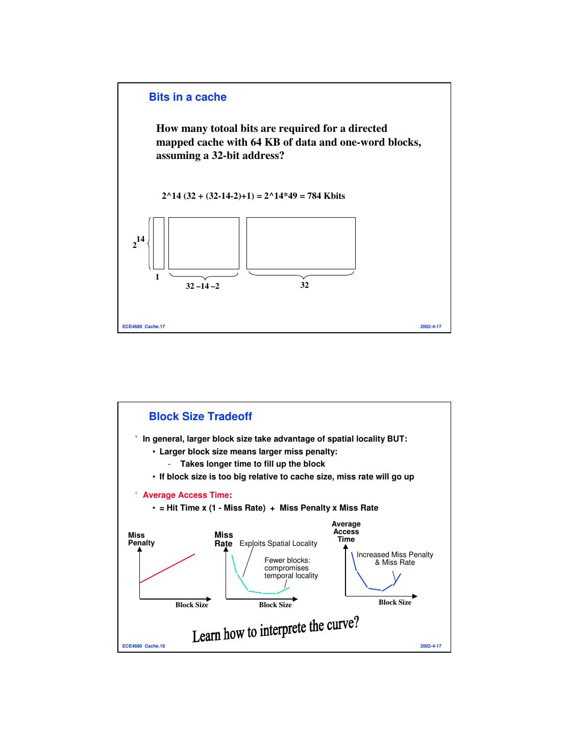
9 . Bits in a cache How many totoal bits are required for a directed mapped cache with 64 KB of data and one-word blocks, assuming a 32-bit address? 2^14 (32 + (32-14-2)+1) = 2^14*49 = 784 Kbits 14 2 1 32 –14 –2 32 ECE4680 Cache.17 2002-4-17 Block Size Tradeoff °In general, larger block size take advantage of spatial locality BUT: • Larger block size means larger miss penalty: - Takes longer time to fill up the block • If block size is too big relative to cache size, miss rate will go up °Average Access Time: • = Hit Time x (1 - Miss Rate) + Miss Penalty x Miss Rate Average Miss Miss Access Penalty Time Rate Exploits Spatial Locality Increased Miss Penalty Fewer blocks: & Miss Rate compromises temporal locality Block Size Block Size Block Size ECE4680 Cache.18 2002-4-17
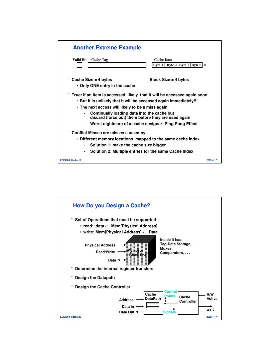
10 . Another Extreme Example Valid Bit Cache Tag Cache Data Byte 3 Byte 2 Byte 1 Byte 0 0 °Cache Size = 4 bytes Block Size = 4 bytes • Only ONE entry in the cache °True: If an item is accessed, likely that it will be accessed again soon • But it is unlikely that it will be accessed again immediately!!! • The next access will likely to be a miss again - Continually loading data into the cache but discard (force out) them before they are used again - Worst nightmare of a cache designer: Ping Pong Effect °Conflict Misses are misses caused by: • Different memory locations mapped to the same cache index - Solution 1: make the cache size bigger - Solution 2: Multiple entries for the same Cache Index ECE4680 Cache.19 2002-4-17 How Do you Design a Cache? °Set of Operations that must be supported • read: data <= Mem[Physical Address] • write: Mem[Physical Address] <= Data Inside it has: Physical Address Tag-Data Storage, Muxes, Read/Write Memory Comparators, . . . “Black Box” Data °Determine the internal register transfers °Design the Datapath °Design the Cache Controller Control Cache Points Cache R/W Address DataPath Active Controller Data In wait Data Out Signals ECE4680 Cache.20 2002-4-17
11 . Impact on Cycle Time PC I -Cache Cache Hit Time: IR directly tied to clock rate miss increases with cache size increases with associativity IRex A B invalid IRm R Average Memory Access time = D Cache Hit Time + Miss Rate x Miss Penalty IRwb T Time = IC x CT x (ideal CPI + memory stalls) Miss ECE4680 Cache.21 2002-4-17 Improving Cache Performance: 3 general options 1. Reduce the miss rate, 2. Reduce the miss penalty, or 3. Reduce the time to hit in the cache. Memory stall cycles = Read stall cycles + write-stall cycles Read stall cycles = #reads * read miss rate * read miss penalty Write stall cycles = #writes * write miss rate * write miss penalty Memory stall cycles = #access * miss rate * miss penalty ECE4680 Cache.22 2002-4-17
12 . Examples: Q1: Assume an instruction cache miss rate for gcc of 2% and a data cache miss rate of 4%. If a machine has a CPI of 2 without any memory stalls and the miss penalty is 40 cycles for all misses, determine how much faster a machine would run with a perfect cache that never missed. (It is known that the frequency of all loads and stores in gcc is 36%, unused) Answer: Instruction miss cycles = I * 2% * 40 = 0.80I Data miss cycles = I * 4% * 40 = 0.56I The CPI with memory stalls is 2 + 1.36 = 3.36 The performance with the perfect cache is better by 1.68 Q2: Suppose we speed up the machine by reducing CPI from 2 to 1. Q3: If we double clock rate, ECE4680 Cache.23 2002-4-17 And yet Another Extreme Example: Fully Associative °Fully Associative Cache • Forget about the Cache Index • Compare the Cache Tags of all cache entries in parallel • Example: Block Size = 32 B blocks, we need N 27-bit comparators °By definition: Conflict Miss = 0 for a fully associative cache 31 4 0 Cache Tag (27 bits long) Byte Select Ex: 0x01 Cache Tag Valid Bit Cache Data : : X Byte 31 Byte 1 Byte 0 X Byte 63 Byte 33 Byte 32 X X X : : : ECE4680 Cache.24 2002-4-17
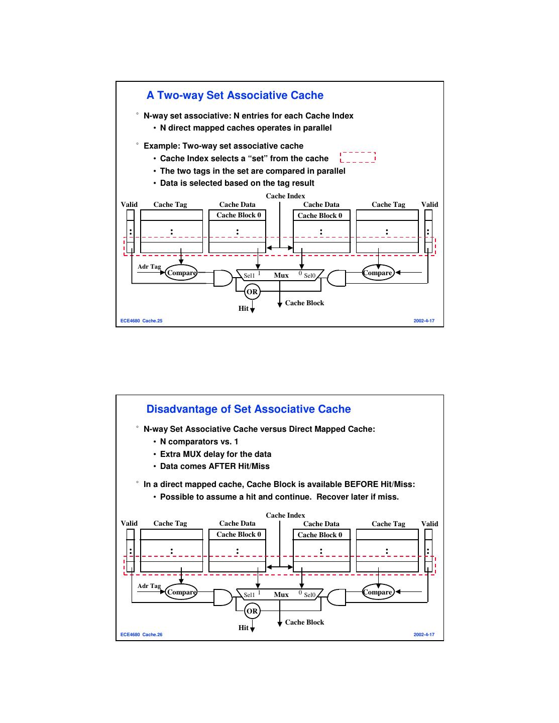
13 . A Two-way Set Associative Cache °N-way set associative: N entries for each Cache Index • N direct mapped caches operates in parallel °Example: Two-way set associative cache • Cache Index selects a “set” from the cache • The two tags in the set are compared in parallel • Data is selected based on the tag result Cache Index Valid Cache Tag Cache Data Cache Data Cache Tag Valid Cache Block 0 Cache Block 0 : : : : : : Adr Tag Compare Sel1 1 Mux 0 Sel0 Compare OR Cache Block Hit ECE4680 Cache.25 2002-4-17 Disadvantage of Set Associative Cache °N-way Set Associative Cache versus Direct Mapped Cache: • N comparators vs. 1 • Extra MUX delay for the data • Data comes AFTER Hit/Miss °In a direct mapped cache, Cache Block is available BEFORE Hit/Miss: • Possible to assume a hit and continue. Recover later if miss. Cache Index Valid Cache Tag Cache Data Cache Data Cache Tag Valid Cache Block 0 Cache Block 0 : : : : : : Adr Tag Compare Sel1 1 Mux 0 Sel0 Compare OR Cache Block Hit ECE4680 Cache.26 2002-4-17
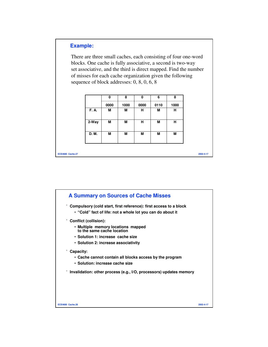
14 . Example: There are three small caches, each consisting of four one-word blocks. One cache is fully associative, a second is two-way set associative, and the third is direct mapped. Find the number of misses for each cache organization given the following sequence of block addresses: 0, 8, 0, 6, 8 0 8 0 6 8 0000 1000 0000 0110 1000 F. A. M M H M H 2-Way M M H M H D. M. M M M M M ECE4680 Cache.27 2002-4-17 A Summary on Sources of Cache Misses °Compulsory (cold start, first reference): first access to a block • “Cold” fact of life: not a whole lot you can do about it °Conflict (collision): • Multiple memory locations mapped to the same cache location • Solution 1: increase cache size • Solution 2: increase associativity °Capacity: • Cache cannot contain all blocks access by the program • Solution: increase cache size °Invalidation: other process (e.g., I/O, processors) updates memory ECE4680 Cache.28 2002-4-17
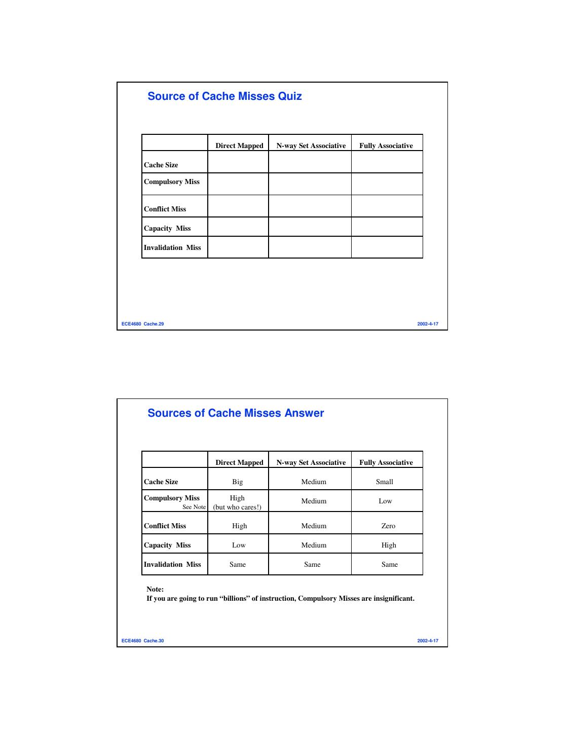
15 . Source of Cache Misses Quiz Direct Mapped N-way Set Associative Fully Associative Cache Size Compulsory Miss Conflict Miss Capacity Miss Invalidation Miss ECE4680 Cache.29 2002-4-17 Sources of Cache Misses Answer Direct Mapped N-way Set Associative Fully Associative Cache Size Big Medium Small Compulsory Miss High Medium Low See Note (but who cares!) Conflict Miss High Medium Zero Capacity Miss Low Medium High Invalidation Miss Same Same Same Note: If you are going to run “billions” of instruction, Compulsory Misses are insignificant. ECE4680 Cache.30 2002-4-17
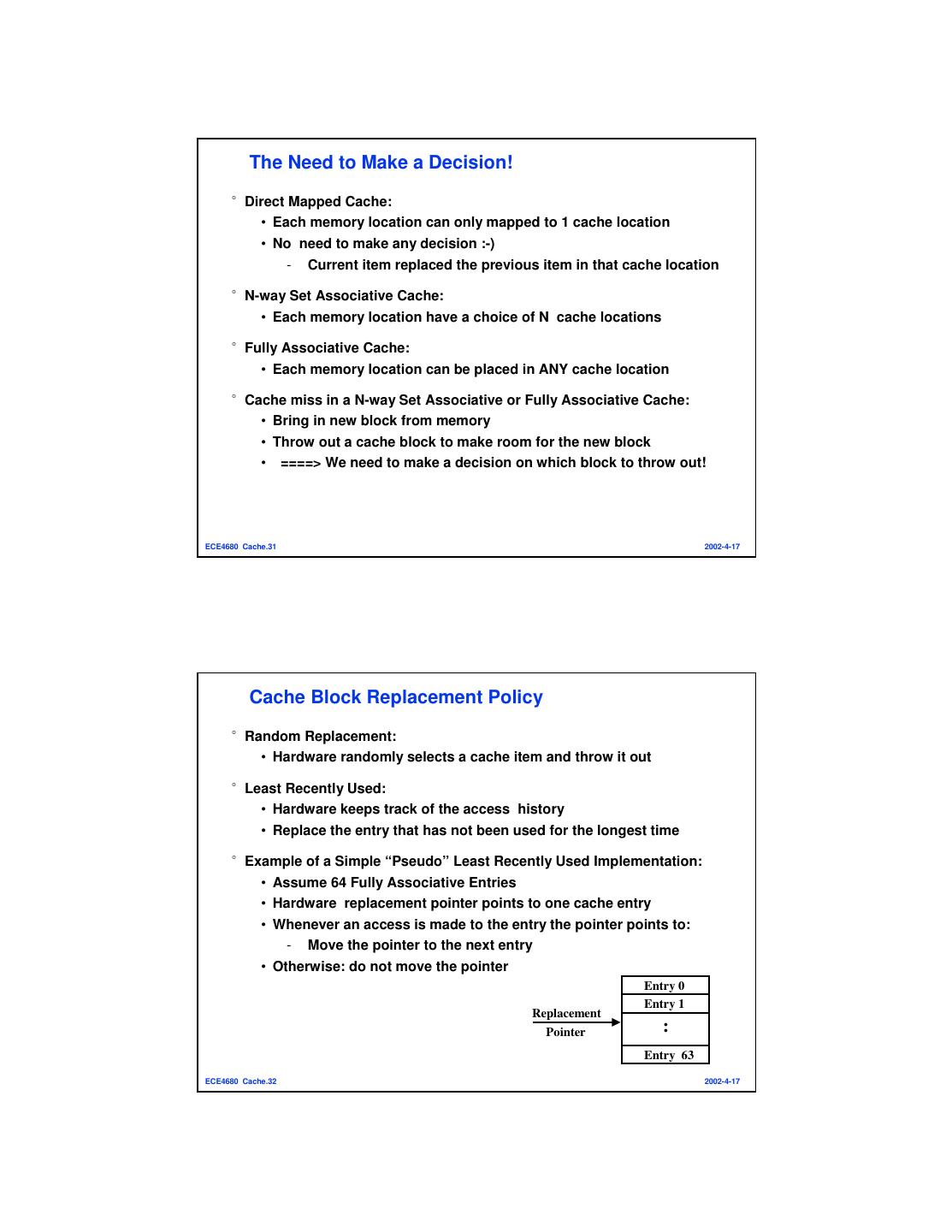
16 . The Need to Make a Decision! °Direct Mapped Cache: • Each memory location can only mapped to 1 cache location • No need to make any decision :-) - Current item replaced the previous item in that cache location °N-way Set Associative Cache: • Each memory location have a choice of N cache locations °Fully Associative Cache: • Each memory location can be placed in ANY cache location °Cache miss in a N-way Set Associative or Fully Associative Cache: • Bring in new block from memory • Throw out a cache block to make room for the new block • ====> We need to make a decision on which block to throw out! ECE4680 Cache.31 2002-4-17 Cache Block Replacement Policy °Random Replacement: • Hardware randomly selects a cache item and throw it out °Least Recently Used: • Hardware keeps track of the access history • Replace the entry that has not been used for the longest time °Example of a Simple “Pseudo” Least Recently Used Implementation: • Assume 64 Fully Associative Entries • Hardware replacement pointer points to one cache entry • Whenever an access is made to the entry the pointer points to: - Move the pointer to the next entry • Otherwise: do not move the pointer Entry 0 Entry 1 Replacement Pointer : Entry 63 ECE4680 Cache.32 2002-4-17
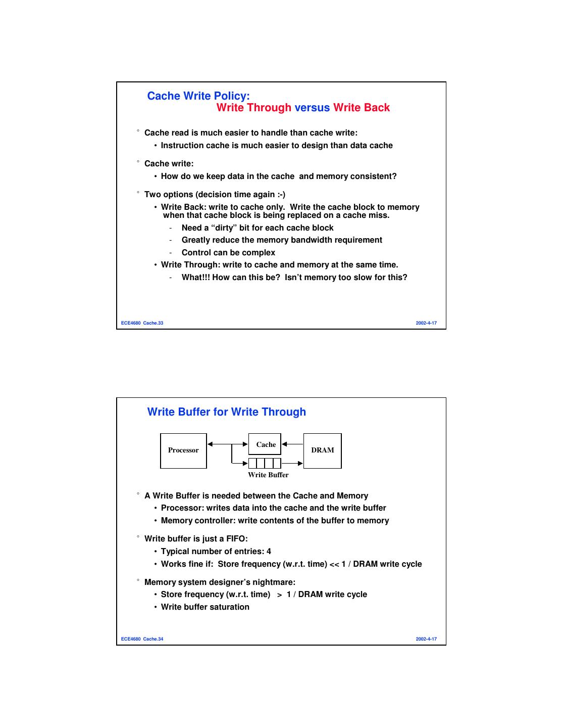
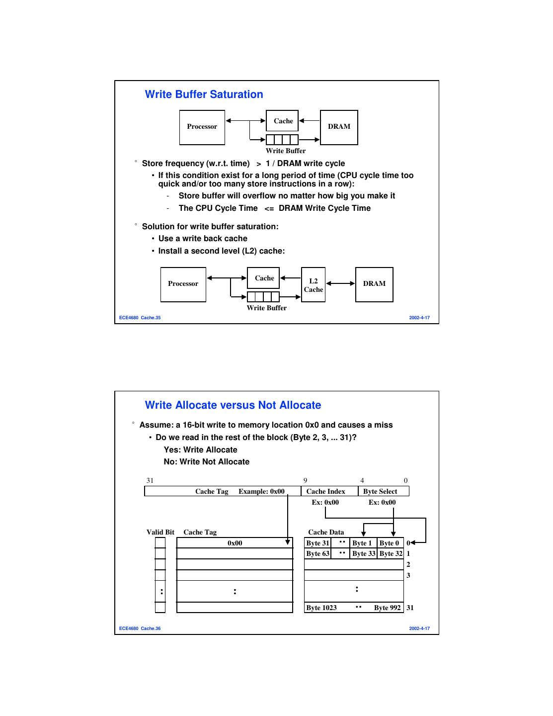
17 . Cache Write Policy: Write Through versus Write Back °Cache read is much easier to handle than cache write: • Instruction cache is much easier to design than data cache °Cache write: • How do we keep data in the cache and memory consistent? °Two options (decision time again :-) • Write Back: write to cache only. Write the cache block to memory when that cache block is being replaced on a cache miss. - Need a “dirty” bit for each cache block - Greatly reduce the memory bandwidth requirement - Control can be complex • Write Through: write to cache and memory at the same time. - What!!! How can this be? Isn’t memory too slow for this? ECE4680 Cache.33 2002-4-17 Write Buffer for Write Through Cache Processor DRAM Write Buffer °A Write Buffer is needed between the Cache and Memory • Processor: writes data into the cache and the write buffer • Memory controller: write contents of the buffer to memory °Write buffer is just a FIFO: • Typical number of entries: 4 • Works fine if: Store frequency (w.r.t. time) << 1 / DRAM write cycle °Memory system designer’s nightmare: • Store frequency (w.r.t. time) > 1 / DRAM write cycle • Write buffer saturation ECE4680 Cache.34 2002-4-17
18 . Write Buffer Saturation Cache Processor DRAM Write Buffer °Store frequency (w.r.t. time) > 1 / DRAM write cycle • If this condition exist for a long period of time (CPU cycle time too quick and/or too many store instructions in a row): - Store buffer will overflow no matter how big you make it - The CPU Cycle Time <= DRAM Write Cycle Time °Solution for write buffer saturation: • Use a write back cache • Install a second level (L2) cache: Cache L2 Processor DRAM Cache Write Buffer ECE4680 Cache.35 2002-4-17 Write Allocate versus Not Allocate °Assume: a 16-bit write to memory location 0x0 and causes a miss • Do we read in the rest of the block (Byte 2, 3, ... 31)? Yes: Write Allocate No: Write Not Allocate 31 9 4 0 Cache Tag Example: 0x00 Cache Index Byte Select Ex: 0x00 Ex: 0x00 Valid Bit Cache Tag Cache Data : : 0x00 Byte 31 Byte 1 Byte 0 0 Byte 63 Byte 33 Byte 32 1 2 3 : : : : Byte 1023 Byte 992 31 ECE4680 Cache.36 2002-4-17
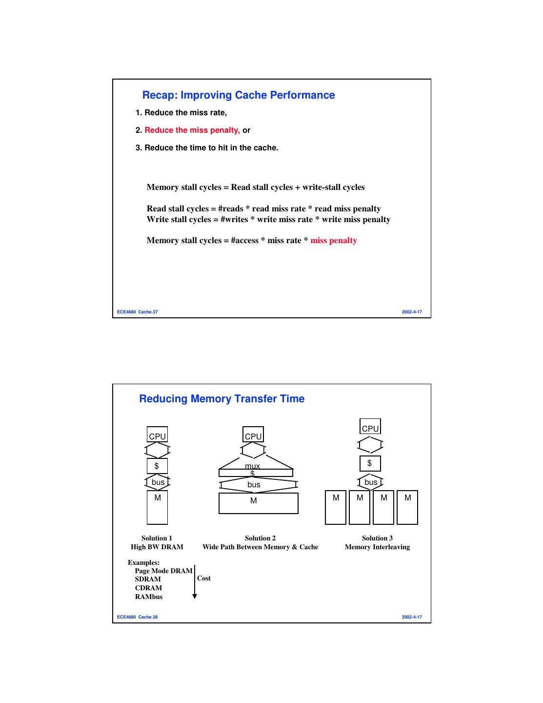
19 . Recap: Improving Cache Performance 1. Reduce the miss rate, 2. Reduce the miss penalty, or 3. Reduce the time to hit in the cache. Memory stall cycles = Read stall cycles + write-stall cycles Read stall cycles = #reads * read miss rate * read miss penalty Write stall cycles = #writes * write miss rate * write miss penalty Memory stall cycles = #access * miss rate * miss penalty ECE4680 Cache.37 2002-4-17 Reducing Memory Transfer Time CPU CPU CPU $ mux $ $ bus bus bus M M M M M M Solution 1 Solution 2 Solution 3 High BW DRAM Wide Path Between Memory & Cache Memory Interleaving Examples: Page Mode DRAM SDRAM Cost CDRAM RAMbus ECE4680 Cache.38 2002-4-17
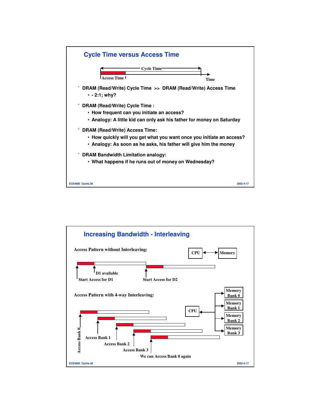
20 . Cycle Time versus Access Time Cycle Time Access Time Time °DRAM (Read/Write) Cycle Time >> DRAM (Read/Write) Access Time • - 2:1; why? °DRAM (Read/Write) Cycle Time : • How frequent can you initiate an access? • Analogy: A little kid can only ask his father for money on Saturday °DRAM (Read/Write) Access Time: • How quickly will you get what you want once you initiate an access? • Analogy: As soon as he asks, his father will give him the money °DRAM Bandwidth Limitation analogy: • What happens if he runs out of money on Wednesday? ECE4680 Cache.39 2002-4-17 Increasing Bandwidth - Interleaving Access Pattern without Interleaving: CPU Memory D1 available Start Access for D1 Start Access for D2 Memory Access Pattern with 4-way Interleaving: Bank 0 Memory Bank 1 CPU Memory Bank 2 Memory Access Bank 0 Bank 3 Access Bank 1 Access Bank 2 Access Bank 3 We can Access Bank 0 again ECE4680 Cache.40 2002-4-17
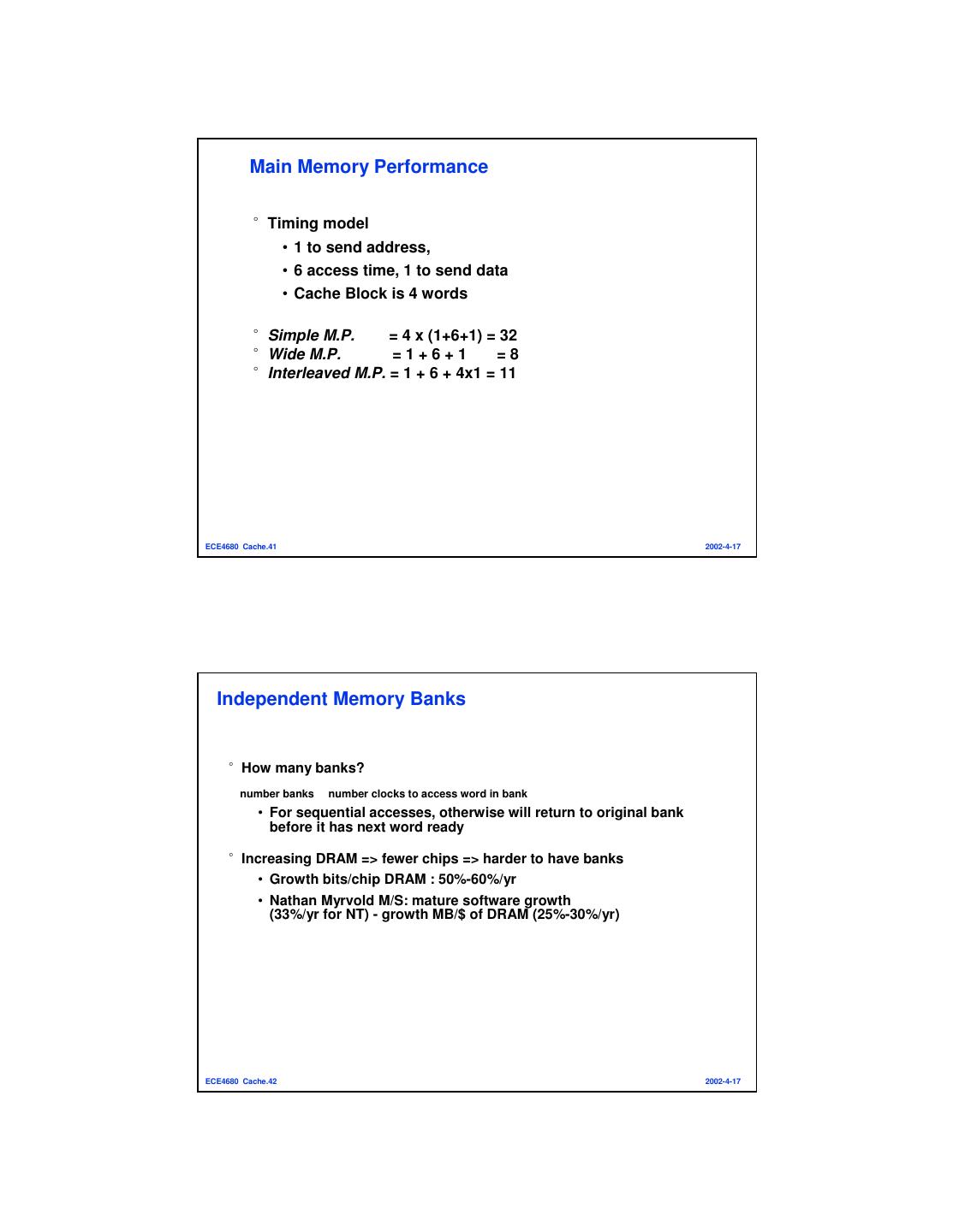
21 . Main Memory Performance °Timing model • 1 to send address, • 6 access time, 1 to send data • Cache Block is 4 words °Simple M.P. = 4 x (1+6+1) = 32 °Wide M.P. =1+6+1 =8 °Interleaved M.P. = 1 + 6 + 4x1 = 11 ECE4680 Cache.41 2002-4-17 Independent Memory Banks °How many banks? number banks number clocks to access word in bank • For sequential accesses, otherwise will return to original bank before it has next word ready °Increasing DRAM => fewer chips => harder to have banks • Growth bits/chip DRAM : 50%-60%/yr • Nathan Myrvold M/S: mature software growth (33%/yr for NT) - growth MB/$ of DRAM (25%-30%/yr) ECE4680 Cache.42 2002-4-17
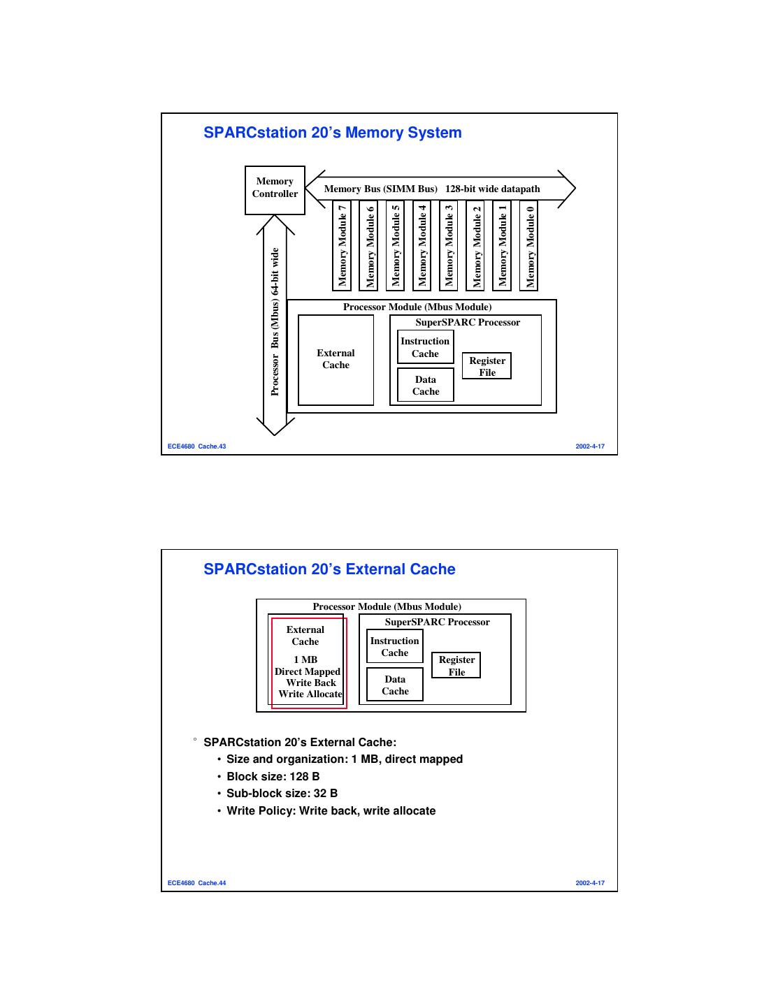
22 . SPARCstation 20’s Memory System Memory Controller Memory Bus (SIMM Bus) 128-bit wide datapath Memory Module 5 Memory Module 4 Memory Module 7 Memory Module 3 Memory Module 1 Memory Module 6 Memory Module 2 Memory Module 0 Processor Bus (Mbus) 64-bit wide Processor Module (Mbus Module) SuperSPARC Processor Instruction External Cache Cache Register File Data Cache ECE4680 Cache.43 2002-4-17 SPARCstation 20’s External Cache Processor Module (Mbus Module) SuperSPARC Processor External Cache Instruction Cache 1 MB Register Direct Mapped File Write Back Data Write Allocate Cache °SPARCstation 20’s External Cache: • Size and organization: 1 MB, direct mapped • Block size: 128 B • Sub-block size: 32 B • Write Policy: Write back, write allocate ECE4680 Cache.44 2002-4-17
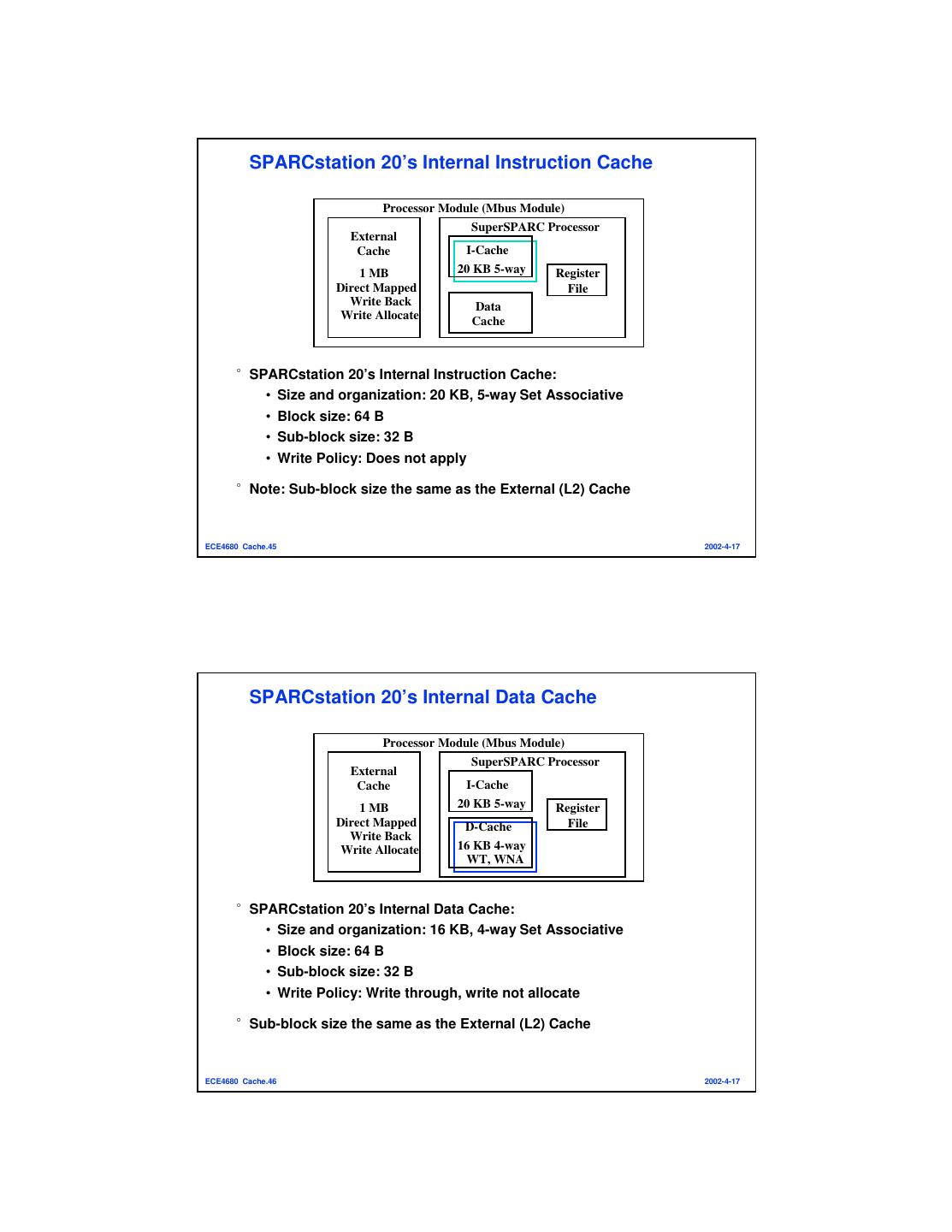
23 . SPARCstation 20’s Internal Instruction Cache Processor Module (Mbus Module) SuperSPARC Processor External Cache I-Cache 1 MB 20 KB 5-way Register Direct Mapped File Write Back Data Write Allocate Cache °SPARCstation 20’s Internal Instruction Cache: • Size and organization: 20 KB, 5-way Set Associative • Block size: 64 B • Sub-block size: 32 B • Write Policy: Does not apply °Note: Sub-block size the same as the External (L2) Cache ECE4680 Cache.45 2002-4-17 SPARCstation 20’s Internal Data Cache Processor Module (Mbus Module) SuperSPARC Processor External Cache I-Cache 1 MB 20 KB 5-way Register Direct Mapped D-Cache File Write Back Write Allocate 16 KB 4-way WT, WNA °SPARCstation 20’s Internal Data Cache: • Size and organization: 16 KB, 4-way Set Associative • Block size: 64 B • Sub-block size: 32 B • Write Policy: Write through, write not allocate °Sub-block size the same as the External (L2) Cache ECE4680 Cache.46 2002-4-17
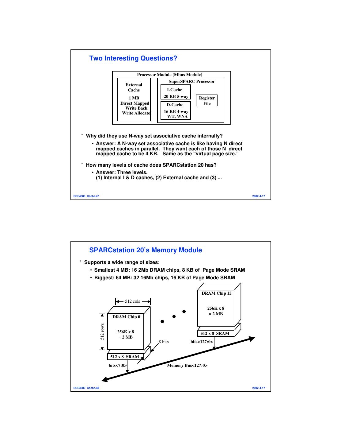
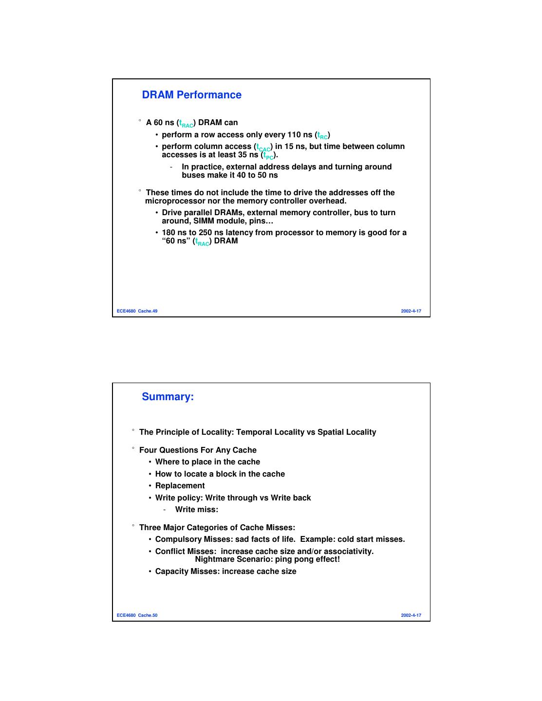
24 . Two Interesting Questions? Processor Module (Mbus Module) SuperSPARC Processor External Cache I-Cache 1 MB 20 KB 5-way Register Direct Mapped D-Cache File Write Back Write Allocate 16 KB 4-way WT, WNA °Why did they use N-way set associative cache internally? • Answer: A N-way set associative cache is like having N direct mapped caches in parallel. They want each of those N direct mapped cache to be 4 KB. Same as the “virtual page size.” °How many levels of cache does SPARCstation 20 has? • Answer: Three levels. (1) Internal I & D caches, (2) External cache and (3) ... ECE4680 Cache.47 2002-4-17 SPARCstation 20’s Memory Module °Supports a wide range of sizes: • Smallest 4 MB: 16 2Mb DRAM chips, 8 KB of Page Mode SRAM • Biggest: 64 MB: 32 16Mb chips, 16 KB of Page Mode SRAM DRAM Chip 15 512 cols 256K x 8 = 2 MB DRAM Chip 0 512 rows 256K x 8 512 x 8 SRAM = 2 MB 8 bits bits<127:0> 512 x 8 SRAM bits<7:0> Memory Bus<127:0> ECE4680 Cache.48 2002-4-17
25 . DRAM Performance °A 60 ns (tRAC) DRAM can • perform a row access only every 110 ns (tRC) • perform column access (tCAC) in 15 ns, but time between column accesses is at least 35 ns (tPC). - In practice, external address delays and turning around buses make it 40 to 50 ns °These times do not include the time to drive the addresses off the microprocessor nor the memory controller overhead. • Drive parallel DRAMs, external memory controller, bus to turn around, SIMM module, pins… • 180 ns to 250 ns latency from processor to memory is good for a “60 ns” (tRAC) DRAM ECE4680 Cache.49 2002-4-17 Summary: °The Principle of Locality: Temporal Locality vs Spatial Locality °Four Questions For Any Cache • Where to place in the cache • How to locate a block in the cache • Replacement • Write policy: Write through vs Write back - Write miss: °Three Major Categories of Cache Misses: • Compulsory Misses: sad facts of life. Example: cold start misses. • Conflict Misses: increase cache size and/or associativity. Nightmare Scenario: ping pong effect! • Capacity Misses: increase cache size ECE4680 Cache.50 2002-4-17
3秒后跳转登录页面
去登陆

