- 快召唤伙伴们来围观吧
- 微博 QQ QQ空间 贴吧
- 文档嵌入链接
- 复制
- 微信扫一扫分享
- 已成功复制到剪贴板
放差分多级大器
展开查看详情
1 .Chapter 6 Differential and Multistage Amplifiers Introduction 6.1 The BJT differntial pair 6.2 Small-signal operation of the BJT differential amplifier 6.3 Other nonideal characteristics of the differential amplifier 6.4 MOS diffenrential amplifiers 6.5 Biasing in intergrated circuits 6.6 The BJT differential amplifier with active load 6.9 Multistage amplifiers
2 .Introduction The differential amplifier (pair) configuration is the most widely used building block in analog IC design. BJT differential amplifier is the basis of a very-high-speed logic circuit family, called emitter-coupled logic (ECL). Why?
3 .Reasons: Direct coupling between signal source and amplifier will easily cause temperature Drift (zero drift). What shall we do?
4 .
5 .Advantages There are 2 reasons for using differential in preference to single-ended amplifiers. (1) Differential circuits are much less sensitive to noise and interference than single-ended circuits. (2) It enables us to bias the amplifier and to couple amplifier stage without the need of bypass and coupling capacitors which are impossible to fabricate economically by IC technology.
6 .6.1 The BJT Differential Pair Basic Operation-1:Common-mode input The differential pair with a common-mode input signal v CM . Two transistors are matched. Current source with infinite output resistance. Current I divide equally between two transistors. The difference in voltage between the two collector is zero. The differential pair rejects the common-mode input signal as long as two transistors remain in active region .
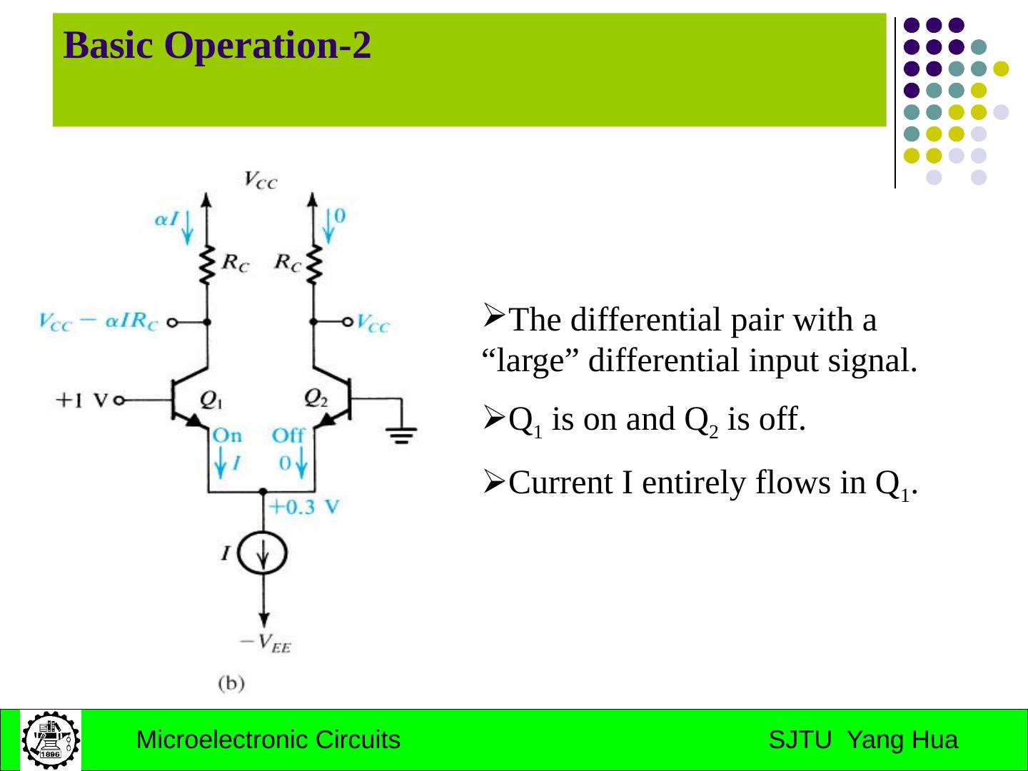
7 .Basic Operation-2 The differential pair with a “large” differential input signal. Q 1 is on and Q 2 is off. Current I entirely flows in Q 1 .
8 .Basic Operation-3 The differential pair with a large differential input signal of polarity opposite to that in (b). Q 2 is on and Q 1 is off. Current I entirely flows in Q 2 .
9 .Basic Operation-4:Difference-mode or Difference signals The differential pair with a small differential input signal v i . Small signal operation or linear amplifier. Assuming the bias current source I to be ideal and thus I remains constant with the change in v CM . Increment in Q 1 and decrement in Q 2 .
10 .Large-Signal Operation
11 .Large-Signal Operation Nonlinear curves. Linear segments. Maximum value of input differential voltages as a small-signal amplifier can be used as a fast current switch Enlarge the linear segment by including equal resistance Re in series with the emitters.
12 .Large-Signal Operation The transfer characteristics of the BJT differential pair (a) can be linearized by including resistances in the emitters.
13 .6.2 Small-signal operation of the BJT differential amplifier The currents and voltages in the differential amplifier when a small differential input signal v id is applied.
14 .A simple technique for determining the signal currents in a differential amplifier excited by a differential voltage signal v id ; dc quantities are not shown. Small-Signal Operation
15 .Small-Signal Operation A differential amplifier with emitter resistances. Only signal quantities are shown (in color).
16 .Input Differential Resistance Input differential resistance is finite. The resistance seen between the two bases is equal to the total resistance in the emitter circuit multiplied by (1+ β). Input differential resistance of differential pair with emitter resistors.
17 .Differential Voltage Gain Differential voltage gain Output voltage taken single-ended Output voltage taken differentially
18 .Differential Voltage Gain Differential voltage gain of the differential pair with resistances in the emitter loads Output voltage taken single-ended Output voltage taken differentially The voltage gain is equal to the ratio of the total resistance in the collector circuit to the total resistance in the emitter circuit.
19 .Differential Half-Circuit Analysis Differential input signals. Single voltage at joint emitters is zero. The circuit is symmetric. Equivalent common-emitter amplifiers in (b).
20 .Differential Half-Circuit Analysis This equivalence applies only for differential input signals. Either of the two common-emitter amplifiers can be used to find the differential gain, differential input resistance, frequency response, and so on Half circuit is biased at I/2. The voltage gain(with the output taken differentially) is equal to the voltage of half circuit.
21 .Differential Half-Circuit Analysis The differential amplifier fed in a single-ended manner . Signal voltage at the emitter is not zero. Almost identical to the symmetric one.
22 .Common-Mode Gain The differential amplifier fed by a common-mode voltage signal v icm .
23 .Common-Mode Gain Equivalent “half-circuits” for common-mode calculations.
24 .Common-Mode Gain Common-mode voltage gain Output voltage taken single-ended Output voltage taken differentially
25 .Common-Mode Rejection Ratio Common-mode rejection ratio Output voltage taken single-ended Output voltage taken differentially This is true only when the circuit is symmetric. Mismatch on CMRR
26 .Input Common-Mode Resistance Definition of the input common-mode resistance R icm . The equivalent common-mode half-circuit.
27 .Input Common-Mode Resistance Input common-mode resistance Input common-mode resistance is very large.
28 .Example 6.1
29 .Example6.1 (cont’d) Evaluate the following: The input differential resistance. The overall differential voltage gain(neglect the effect of r o ). The worst-case common-mode gain if the two collector resistance are accurate within ±1%. The CMRR, in dB. The input common-mode resistance(suppose the Early voltage is 100V).


