- 快召唤伙伴们来围观吧
- 微博 QQ QQ空间 贴吧
- 文档嵌入链接
- 复制
- 微信扫一扫分享
- 已成功复制到剪贴板
19 计算机组成--MIPS处理器的设计(2)
展开查看详情
1 .Design of the MIPS Processor (contd) First, revisit the datapath for add, sub, lw, sw. We will augment it to accommodate the beq and j instructions. Execution of branch instructions beq $at, $zero, L add $v1, $v0, $zero add $v1, $v1, $v1 j somewhere L: add $v1, $v0, $v0 Offset= 3x4=12 The offset must be added to the next PC to generate the target address for branch.
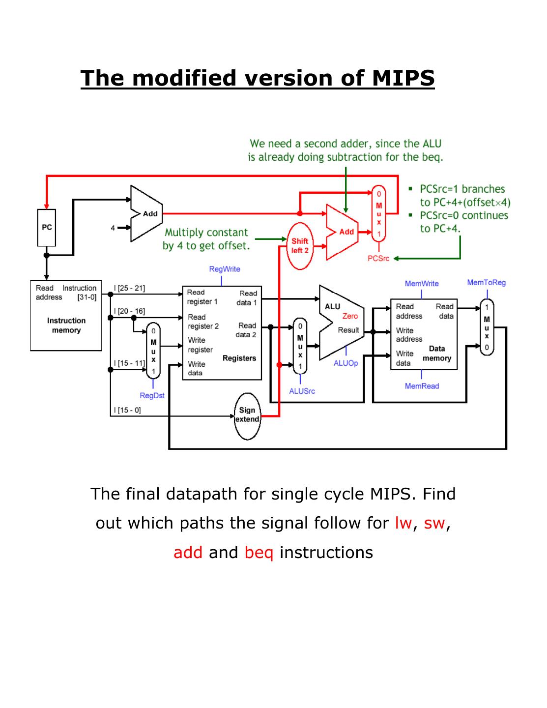
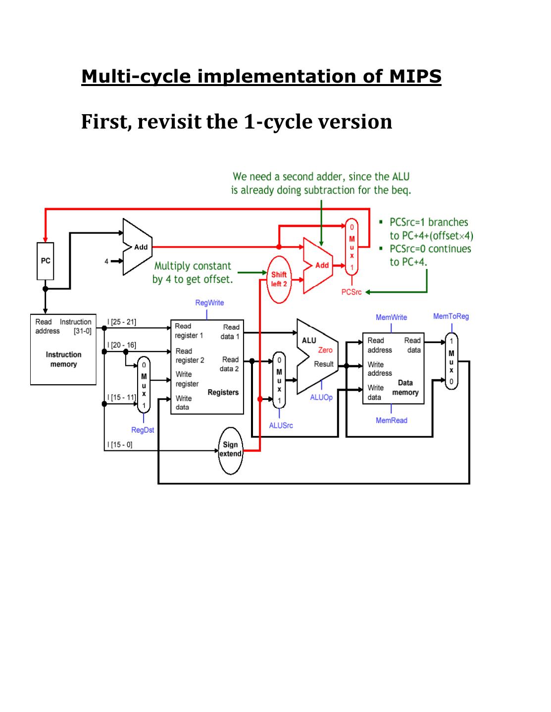
2 .The modified version of MIPS The final datapath for single cycle MIPS. Find out which paths the signal follow for lw, sw, add and beq instructions
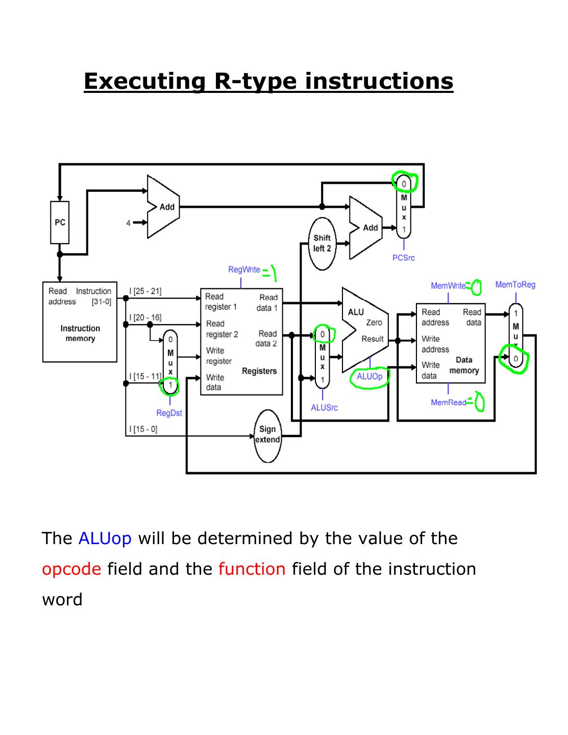
3 . Executing R-type instructions The ALUop will be determined by the value of the opcode field and the function field of the instruction word
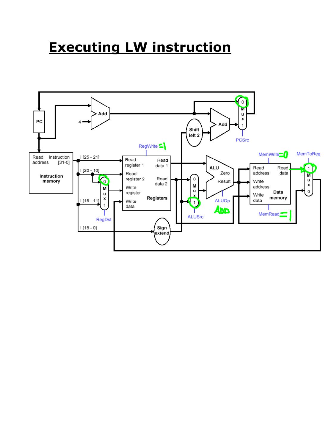
4 .Executing LW instruction
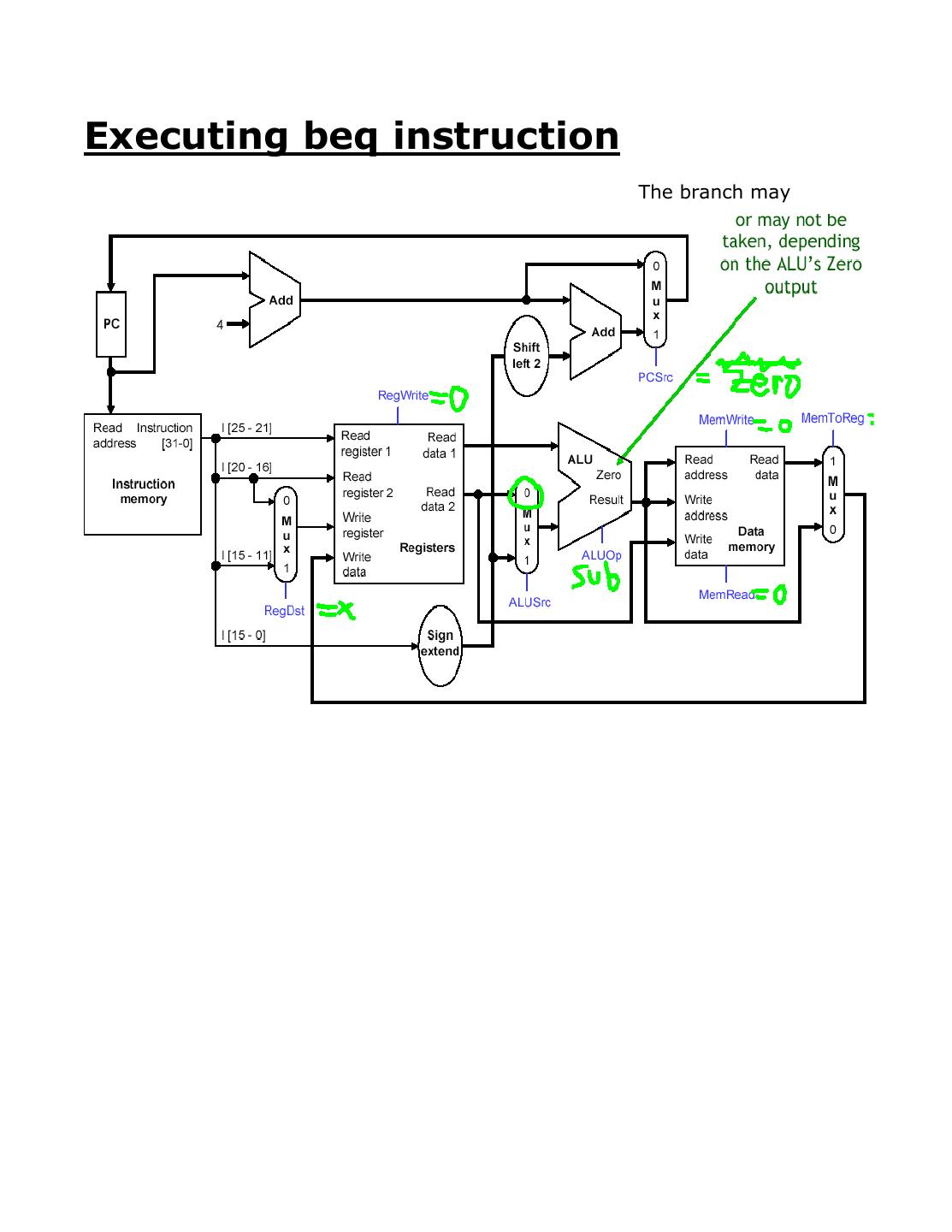
5 .Executing beq instruction The branch may
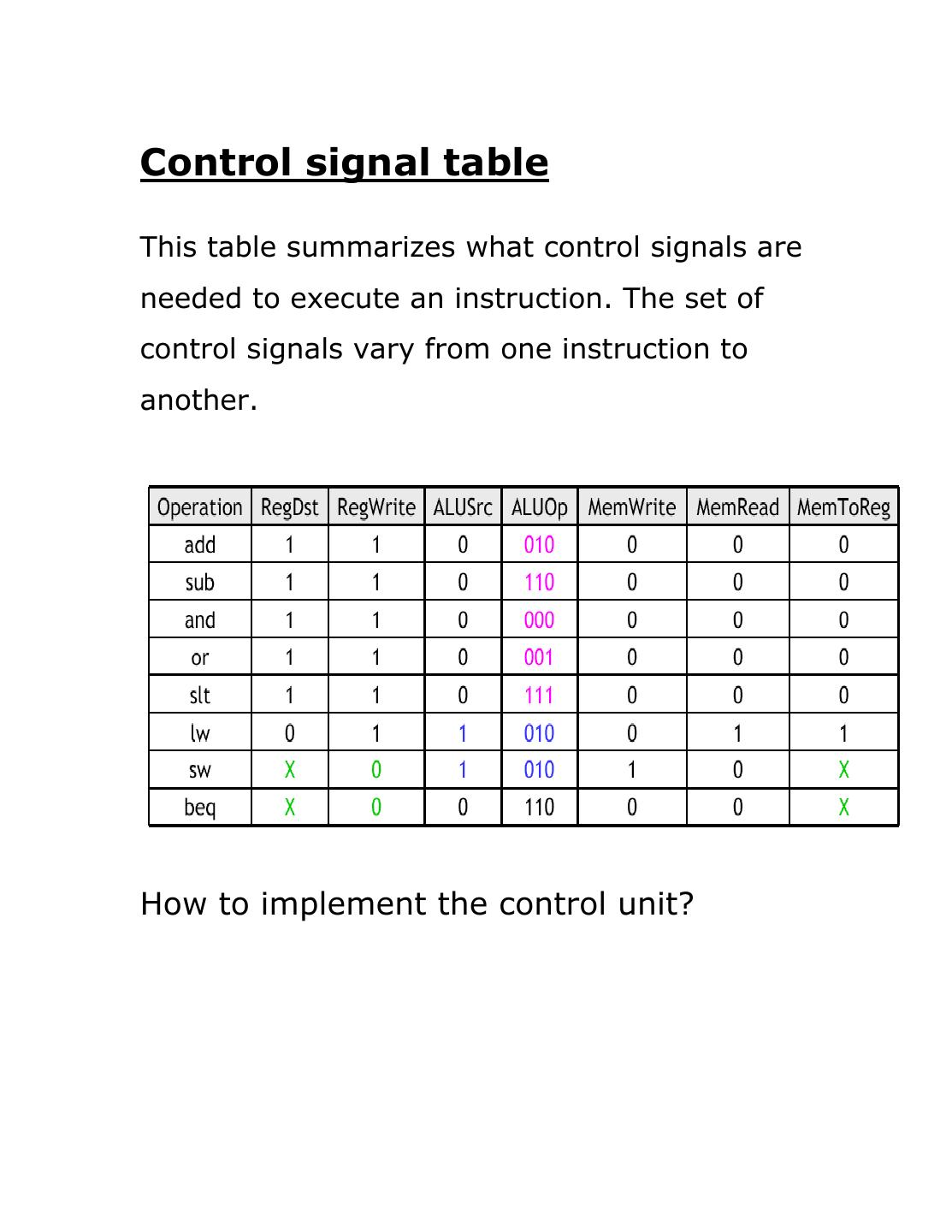
6 .Control signal table This table summarizes what control signals are needed to execute an instruction. The set of control signals vary from one instruction to another. How to implement the control unit?
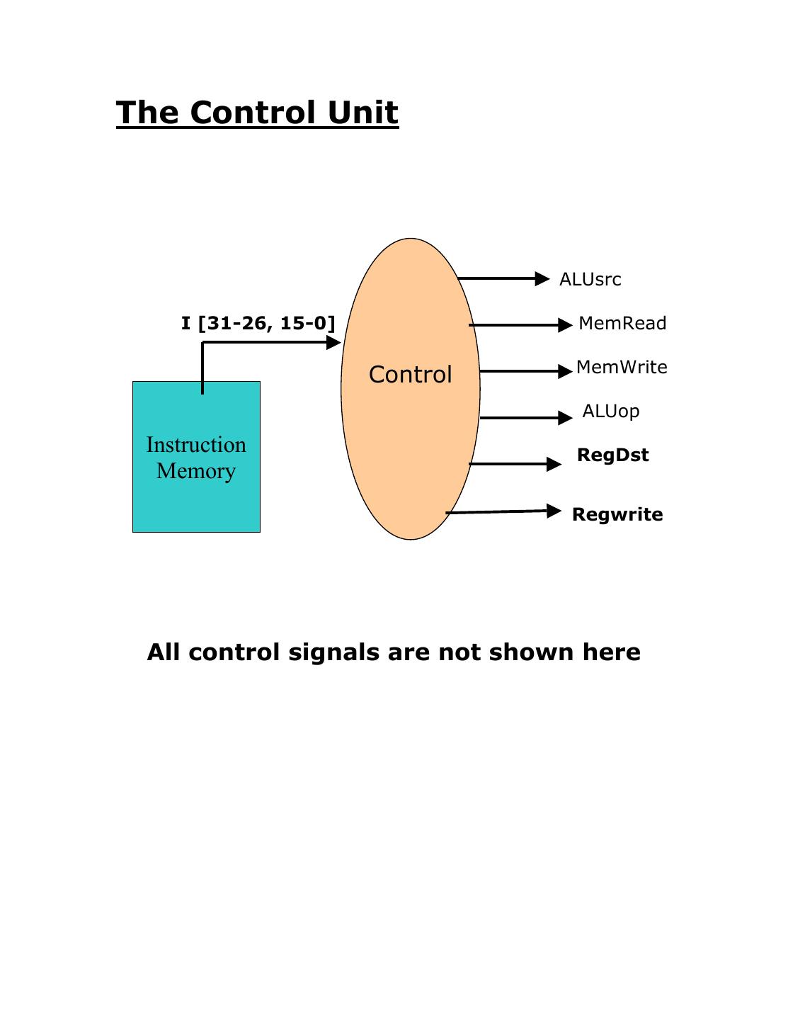
7 .The Control Unit ALUsrc I [31-26, 15-0] MemRead MemWrite Control ALUop Instruction RegDst Memory Regwrite All control signals are not shown here
8 . 1-cycle implementation is not used Why? Because the length of the clock cycle will always be determined by the slowest operation (lw, sw) even when the data memory is not used. Practical implementations use multiple cycles per instruction, which fixes some shortcomings of the 1-cycle implementation. Faster instructions are not held back by the slower instructions The clock cycle time can be decreased. Eventually simplifies the implementation of pipelining, the universal speed-up technique This requires some changes in the datapath
9 .Multi-cycle implementation of MIPS !"#$%&'#()"$"%'%*('+,-.-/(')(#$"01''
10 .The multi-cycle version Note that we have eliminated two adders, and used only one memory unit (so it is Princeton architecture) that contains both instructions and data. It is not essential to have a single memory unit, but it shows an alternative design of the datapath.
11 . Intermediate registers are necessary In each cycle, a fraction of the instruction is executed Five stages of instruction execution Cycle 1. Instruction fetch and PC increment !"#$%&'(&&)%*+,-.&/012#%/&3204&56%&2%.,/5%2&3,$%&&& Cycle 3 Performing an ALU computation Cycle 4 Reading or writing (data) memory Cycle 5 Storing data back to the register file
12 .Why intermediate registers? Sometimes we need the output of a functional unit in a later clock cycle during the execution of an instruction. (Example: The instruction word fetched in stage 1 determines the destination of the register write in stage 5. The ALU result for an address computation in stage 3 is needed as the memory address for lw or sw in stage 4.) These outputs must be stored in intermediate registers for future use. Otherwise they will be lost by the next clock cycle. (Instruction read in stage 1 is saved in Instruction register. Register file outputs from stage 2 are saved in registers A and B. The ALU output will be stored in a register ALUout. Any data fetched from memory in stage 4 is kept in the Memory data register MDR.)
13 .The Five Cycles of MIPS (Instruction Fetch) IR:= Memory[PC] PC:= PC+4 (Instruction decode and Register fetch) A:= Reg[IR[25:21]], B:=Reg[IR[20:16]] ALUout := PC + sign-extend(IR[15:0]] (Execute|Memory address|Branch completion) Memory reference: ALUout:= A+ IR[15:0] R-type (ALU): ALUout:= A op B Branch: if A=B then PC := ALUout (Memory access | R-type completion) LW: MDR:= Memory[ALUout] SW: Memory[ALUout]:= B R-type: Reg[IR[15:11]]:= ALUout (Writeback) LW: Reg[[20:16]]:= MDR


