- 快召唤伙伴们来围观吧
- 微博 QQ QQ空间 贴吧
- 文档嵌入链接
- 复制
- 微信扫一扫分享
- 已成功复制到剪贴板
15计算机组成--内存
展开查看详情
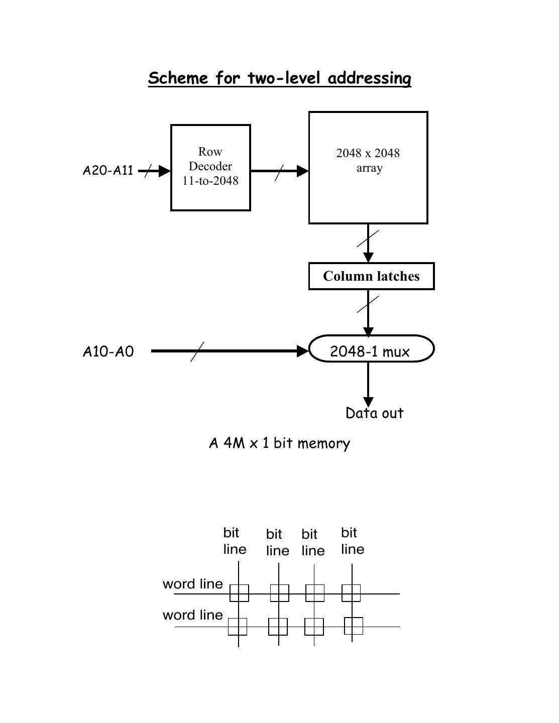
1 . Inside RAM Two-level addressing Consider a 4M x 1 bit RAM. It will apparently need a 22- to-4M decoder. 4 million output lines will make it complex! Complex! Tw0-level addressing simplifies it. These are D flip-flops A21-A0 Din Dout 22 – to-222 decoder In two-level addressing, the memory cells for any bit position are logically arranged as a two-dimensional array. 11 address lines are used to select a row, and 11 address lines are used to select a column. This reduces the number of output lines of the decoders from 4M to 2048 + 2048 = 4096 only.
2 . Basic idea 0 1 0 1 2 3 4 5 6 7 2 8 9 10 11 12 13 14 15 3 16 17 18 19 20 21 22 23 24 25 26 27 28 29 30 31 32 33 34 35 36 37 38 39 40 41 42 43 44 45 46 47 48 49 50 51 52 53 54 55 56 57 58 59 60 61 62 63 A 3-to-8 decoder for row A 3-to-8 decoder for the column (8+8=16 wires lead to the memory) 60 61 62 A 6-to-64 decoder will decode the address 63 (64 wires lead to the memory cells)
3 . Scheme for two-level addressing Row 2048 x 2048 A20-A11 Decoder array 11-to-2048 Column latches A10-A0 2048-1 mux Data out A 4M x 1 bit memory bit bit bit bit line line line line word line word line
4 .Modified scheme with shared address lines To save pins, in 4M x1 bit DRAMs, 11 common lines are used for both A20-A11 and A10-A0. A pair of signals (RAS = Row Access Strobe and CAS = Column Access Strobe) notify which part of the address is present at the input lines.
5 . Dynamic RAM Word line A bit is stored Bit line (data) here as charge on the capacitor Ground A “1” in the word line closes the switch, and the input data through the bit line charges the capacitor. During reading, the voltage on the capacitor is sensed through the bit line to determine if the content is a “1” or a “0”. To safeguard the leakage of the capacitor, it is periodically refreshed (An entire row in one cycle). Very high packing density, but slow (45-65 ns access time) DRAM is a good choice for the main memory.
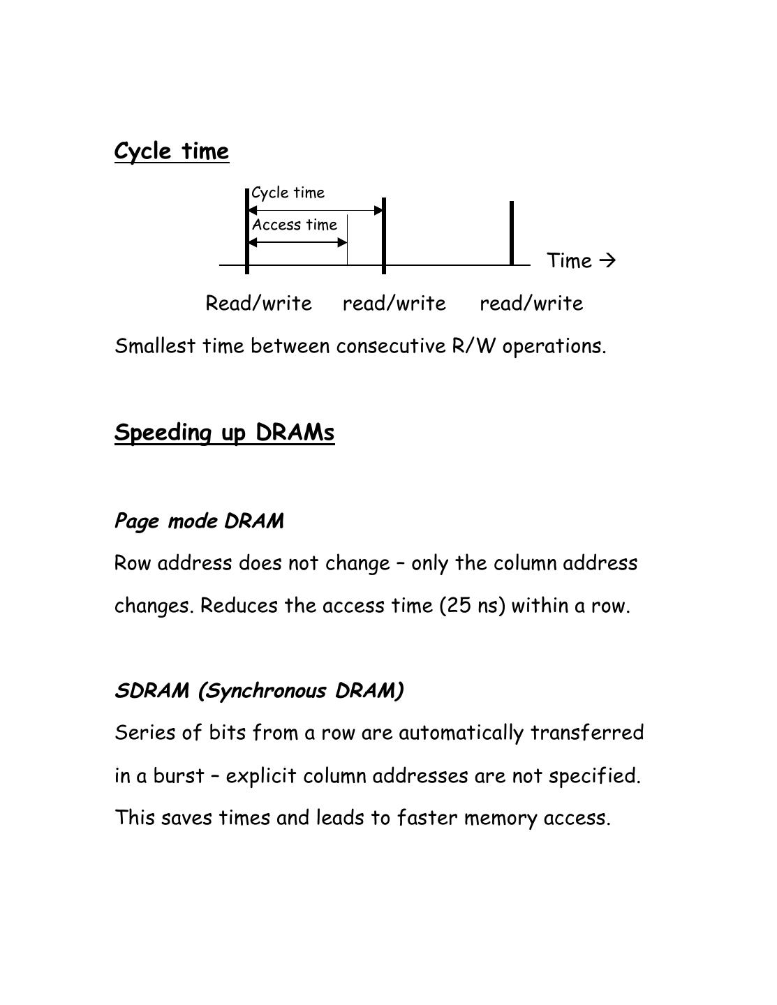
6 .Cycle time Cycle time Access time Time Read/write read/write read/write Smallest time between consecutive R/W operations. Speeding up DRAMs Page mode DRAM Row address does not change – only the column address changes. Reduces the access time (25 ns) within a row. SDRAM (Synchronous DRAM) Series of bits from a row are automatically transferred in a burst – explicit column addresses are not specified. This saves times and leads to faster memory access.
7 .ROM and PLA and FPGA ROM = Read Only Memory PLA = Programmable Logic Array FPGA = Field Programmable Gate Array Here a ROM that is a solid-state device (not an electro- mechanical device like a CD-ROM). Its contents can be randomly accessed, very similar to RAM, with the exception that it contains fixed codes/data that cannot be erased or overwritten by the programmer. Needs special equipment to write data into it. Some can be programmed only once, and often done at the factory. In the programmable variety of ROMs (PROM), the contents can be erased (by ultraviolet radiation or electrical pulses as in EEPROM) and reprogrammed.
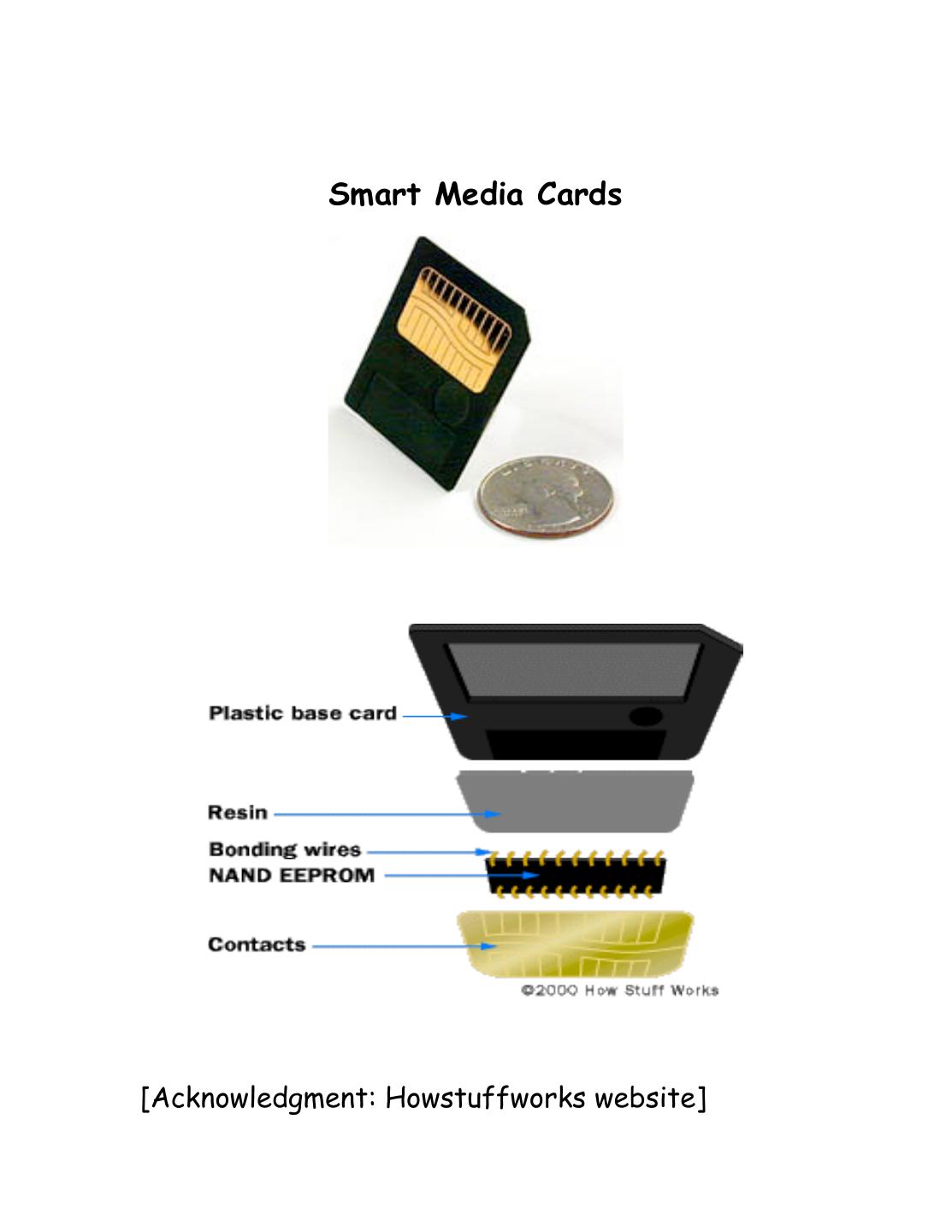
8 .Flash Memory Flash Memory is a form of EEPROM (Electrically Erasable Programmable ROM). Extensively used in USB thumb drives, memory sticks etc. Smart Media and Compact Flash are used as electronic films in digital cameras. Flash memory works much faster than traditional EEPROMs because instead of erasing one byte at a time, it erases a block or the entire chip, and then rewrites it.
9 . Smart Media Cards [Acknowledgment: Howstuffworks website]
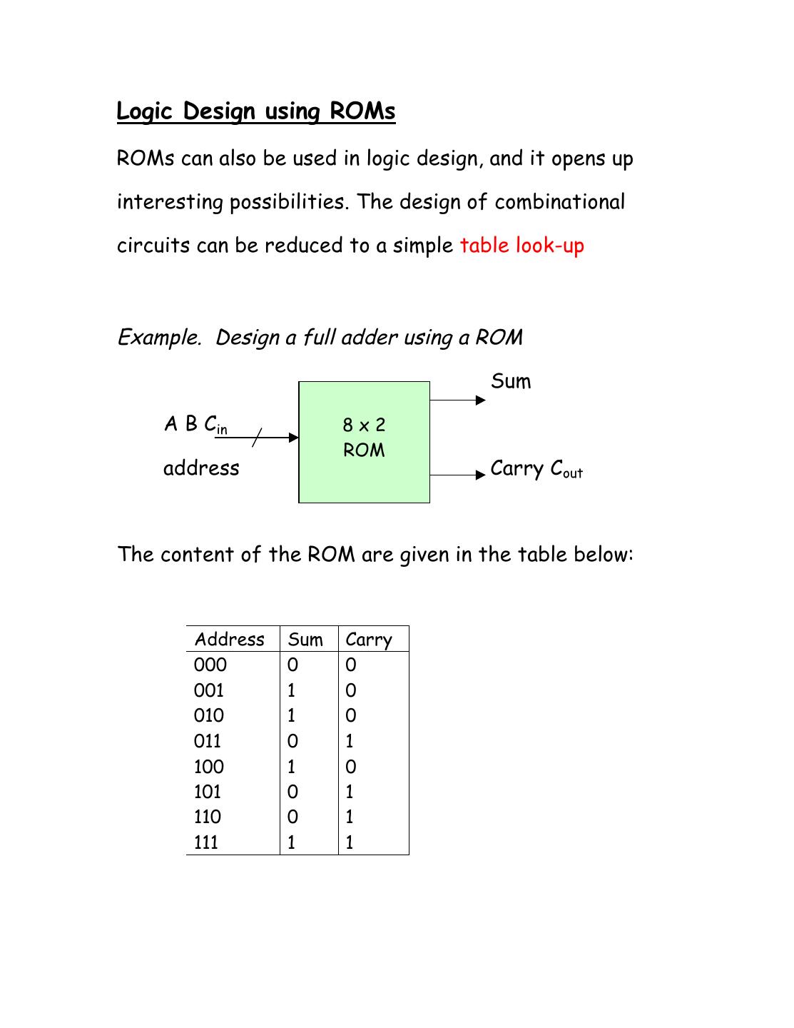
10 .Logic Design using ROMs ROMs can also be used in logic design, and it opens up interesting possibilities. The design of combinational circuits can be reduced to a simple table look-up Example. Design a full adder using a ROM Sum A B Cin 8x2 ROM address Carry Cout The content of the ROM are given in the table below: Address Sum Carry 000 0 0 001 1 0 010 1 0 011 0 1 100 1 0 101 0 1 110 0 1 111 1 1
11 .FPGA (Field Programmable Gate Array) FPGA is a semiconductor device containing programmable logic components and programmable interconnects. Logic blocks can be programmed to perform the function of basic logic gates such as AND, and XOR, or more complex combinational functions such as decoders or mathematical functions. In most FPGAs, the logic blocks also include memory elements, which may be simple flip-flops or more complete blocks of memory. It is a useful building block for prototyping hardware design.
12 .


