14 计算机组成--寄存器文件结构
分享
点赞
0
收藏
1
下载 0
-
快召唤伙伴们来围观吧
-
微博
QQ
QQ空间
贴吧
-
文档嵌入链接
- 复制
-
-
微信扫一扫分享
-
已成功复制到剪贴板
 王木木
王木木
/
发布于
/
2124
人观看
本篇文档主要介绍了寄存器文件结构,具体介绍了创建读取端口、创建写端口、主存、SRAM的典型大小、用4片8K x 1 bit 的 RAM 连接成32K x 1 bit 的RAM 、 用 32K x 1 bit 的RAM 连接成32Kx 4 bit RAM。
展开查看详情
1 .Register file construction
Creating read ports
�
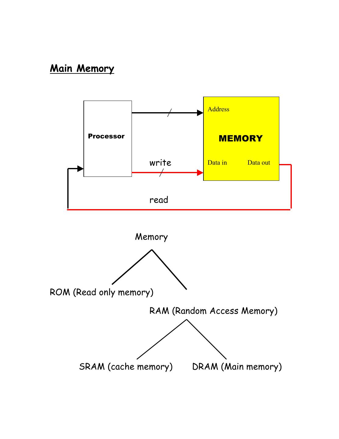
3 .Main Memory
Address
Processor MEMORY
write Data in Data out
read
Memory
ROM (Read only memory)
RAM (Random Access Memory)
SRAM (cache memory) DRAM (Main memory)
�
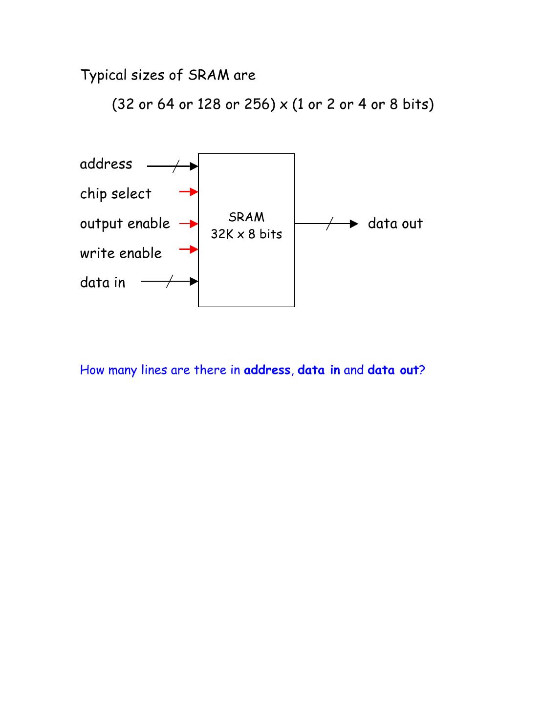
4 .Typical sizes of SRAM are
(32 or 64 or 128 or 256) x (1 or 2 or 4 or 8 bits)
address
chip select
SRAM
output enable data out
32K x 8 bits
write enable
data in
How many lines are there in address, data in and data out?
�
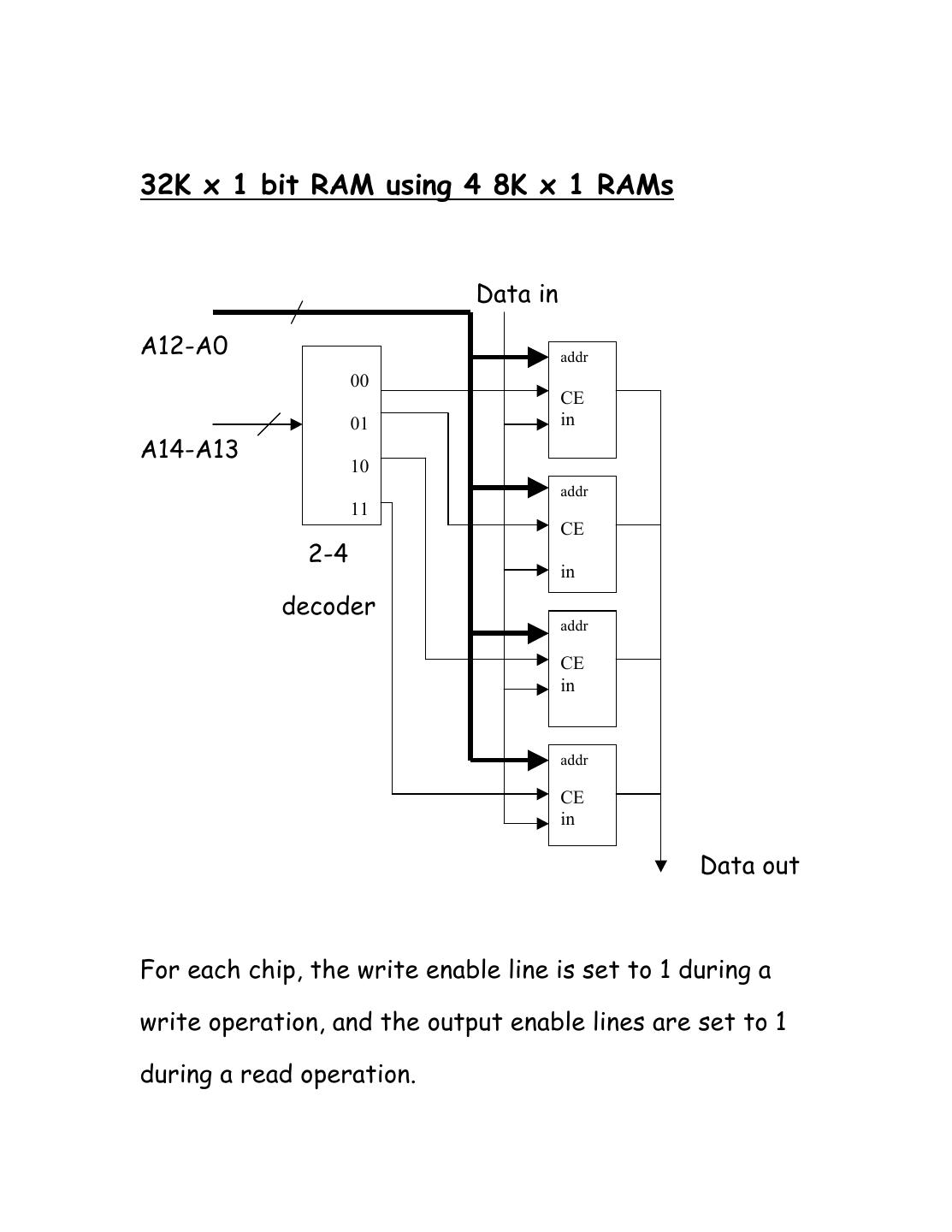
6 .32K x 1 bit RAM using 4 8K x 1 RAMs
Data in
A12-A0 addr
00
CE
01 in
A14-A13
10
addr
11
CE
2-4
in
decoder
addr
CE
in
addr
CE
in
Data out
For each chip, the write enable line is set to 1 during a
write operation, and the output enable lines are set to 1
during a read operation.
�
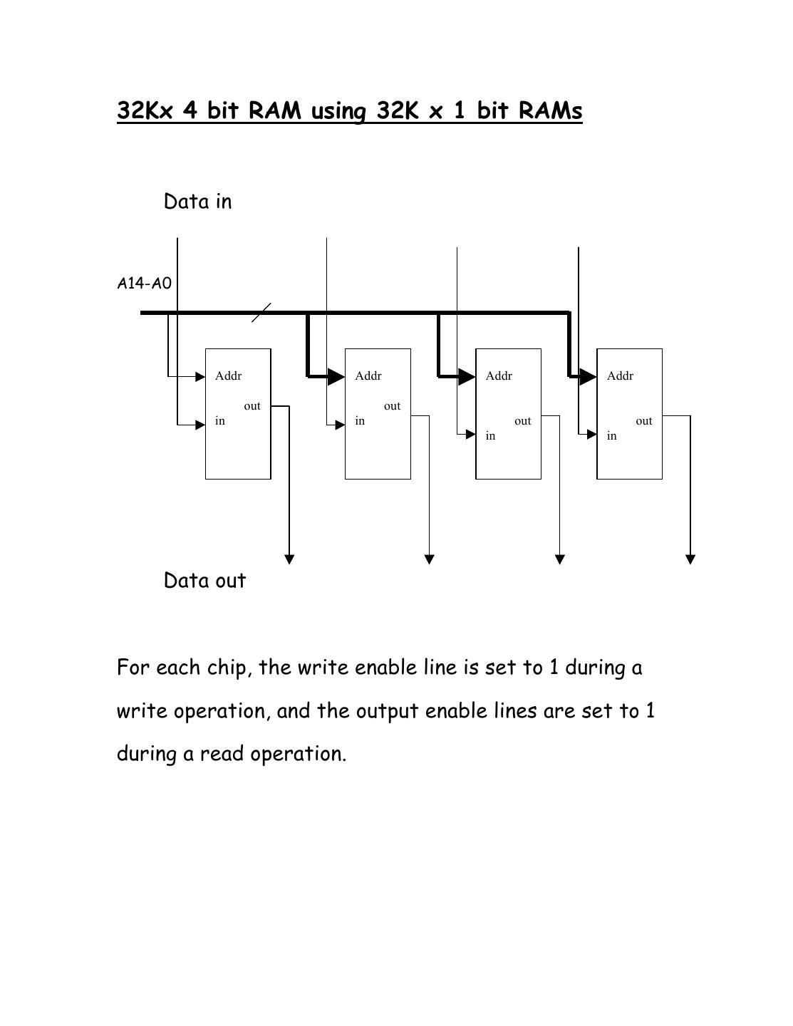
7 .32Kx 4 bit RAM using 32K x 1 bit RAMs
Data in
A14-A0
Addr Addr Addr Addr
out out
in in out out
in in
Data out
For each chip, the write enable line is set to 1 during a
write operation, and the output enable lines are set to 1
during a read operation.
�