- 快召唤伙伴们来围观吧
- 微博 QQ QQ空间 贴吧
- 文档嵌入链接
- 复制
- 微信扫一扫分享
- 已成功复制到剪贴板
13 计算机组成--时序电路
展开查看详情
1 .Sequential Circuits The output depends not only on the current inputs, but also on the past values of the inputs. This is how a digital circuit remembers data. Let us see ho a single bit is stored. R Q An SR Latch S Q R = Reset, S= Set S R Q Q Comment 0 0 0/1 1/0 Old state continues 1 0 1 0 Set state 0 1 0 1 Reset state 1 1 0 0 Illegal inputs
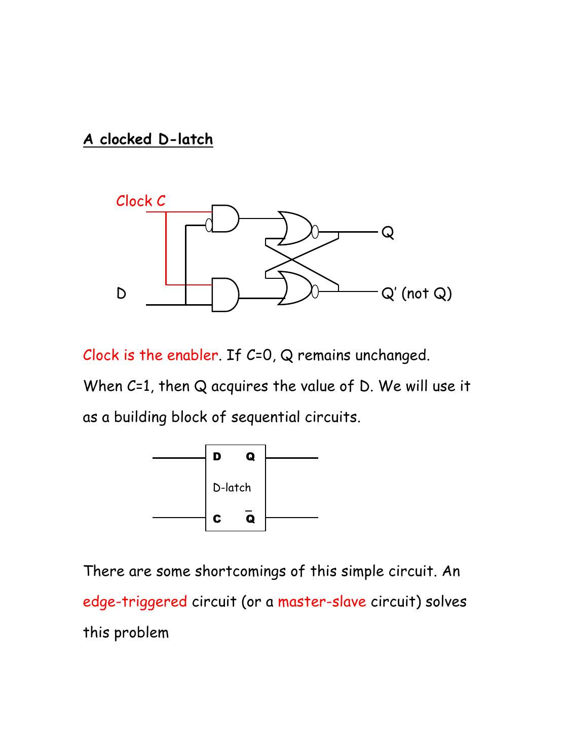
2 .A clocked D-latch Clock C Q D Q’ (not Q) Clock is the enabler. If C=0, Q remains unchanged. When C=1, then Q acquires the value of D. We will use it as a building block of sequential circuits. D Q D-latch C Q There are some shortcomings of this simple circuit. An edge-triggered circuit (or a master-slave circuit) solves this problem
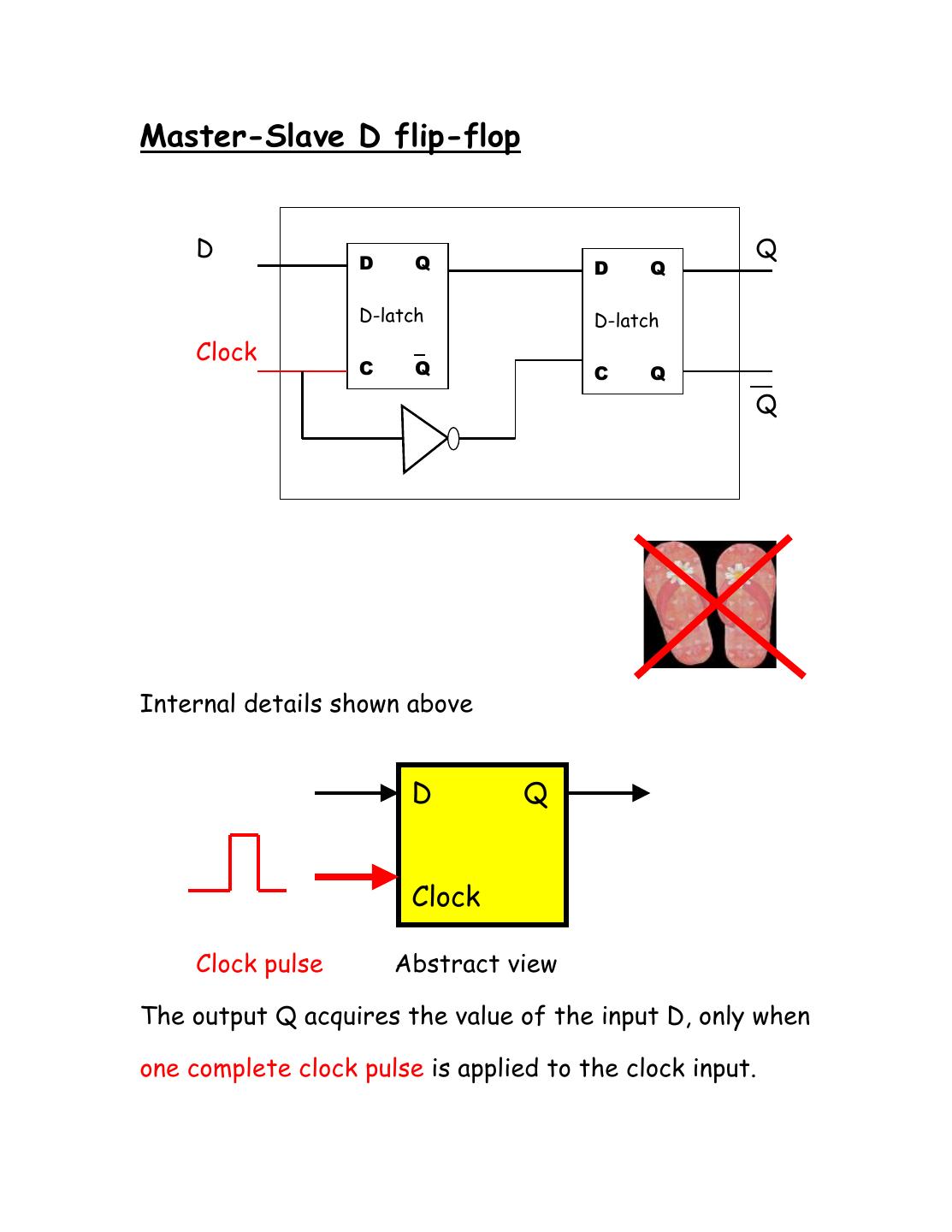
3 .Master-Slave D flip-flop D Q D Q D Q D-latch D-latch Clock C Q C Q Q Internal details shown above D Q Clock Clock pulse Abstract view The output Q acquires the value of the input D, only when one complete clock pulse is applied to the clock input.
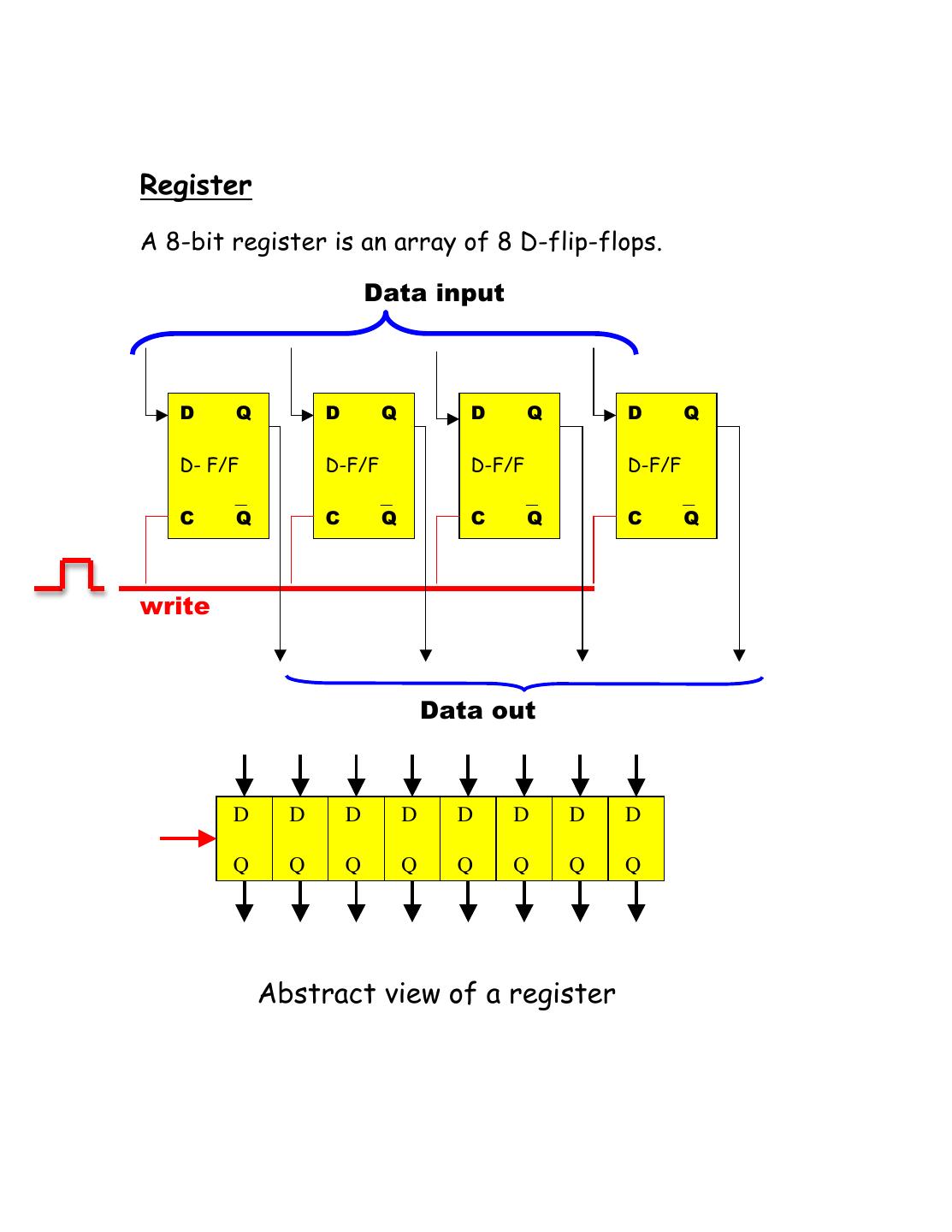
4 .Register A 8-bit register is an array of 8 D-flip-flops. Data input D Q D Q D Q D Q D- F/F D-F/F D-F/F D-F/F C Q C Q C Q C Q write Data out D D D D D D D D Q Q Q Q Q Q Q Q Abstract view of a register
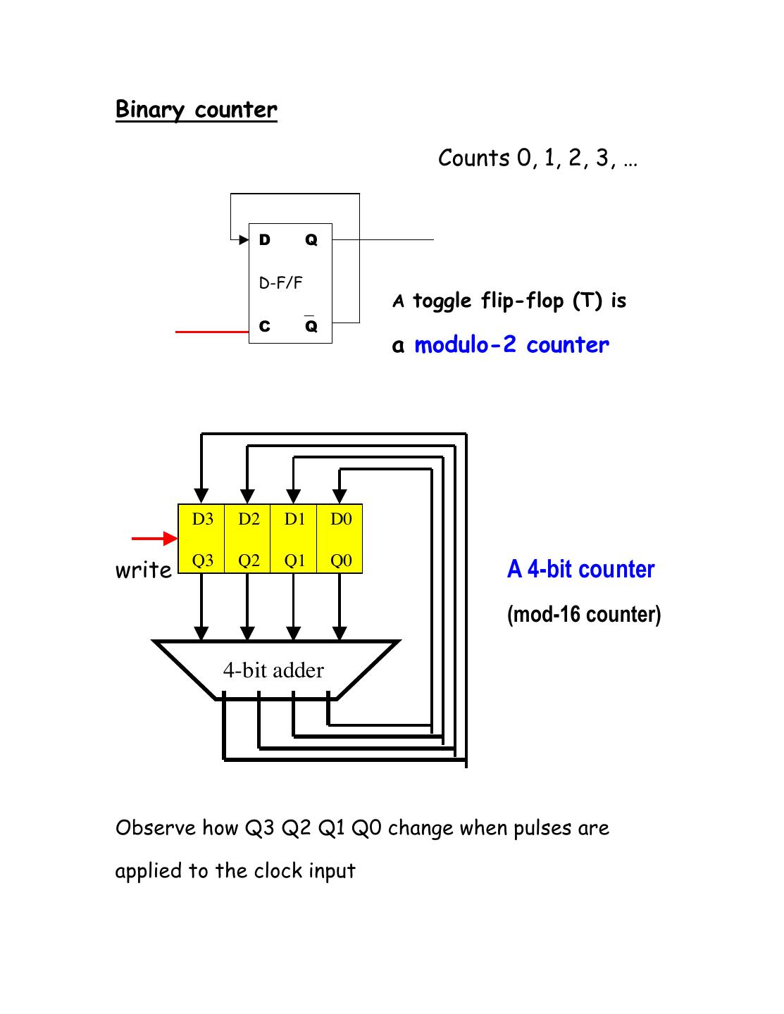
5 .Binary counter Counts 0, 1, 2, 3, … D Q D-F/F A toggle flip-flop (T) is C Q a modulo-2 counter D3 D2 D1 D0 write Q3 Q2 Q1 Q0 A 4-bit counter (mod-16 counter) 4-bit adder Observe how Q3 Q2 Q1 Q0 change when pulses are applied to the clock input
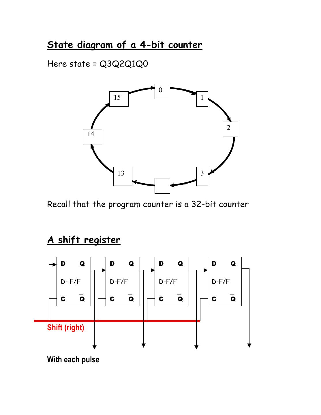
6 .State diagram of a 4-bit counter Here state = Q3Q2Q1Q0 0 15 1 2 14 13 3 Recall that the program counter is a 32-bit counter A shift register D Q D Q D Q D Q D- F/F D-F/F D-F/F D-F/F C Q C Q C Q C Q Shift (right) With each pulse
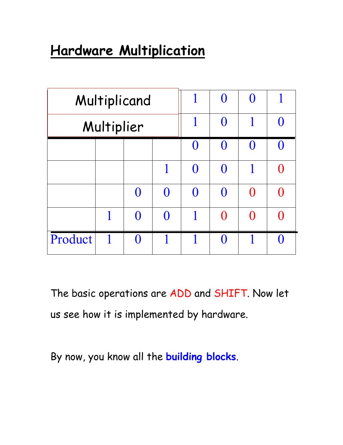
7 .Hardware Multiplication Multiplicand 1 0 0 1 Multiplier 1 0 1 0 0 0 0 0 1 0 0 1 0 0 0 0 0 0 0 1 0 0 1 0 0 0 Product 1 0 1 1 0 1 0 The basic operations are ADD and SHIFT. Now let us see how it is implemented by hardware. By now, you know all the building blocks.
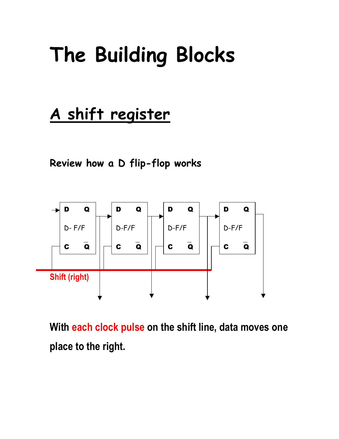
8 .The Building Blocks A shift register Review how a D flip-flop works D Q D Q D Q D Q D- F/F D-F/F D-F/F D-F/F C Q C Q C Q C Q Shift (right) With each clock pulse on the shift line, data moves one place to the right.
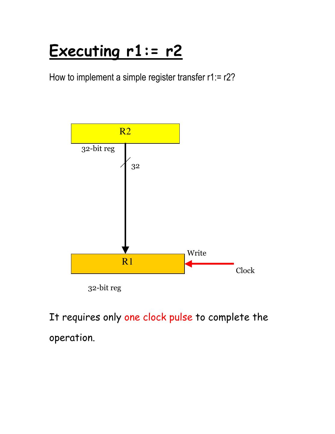
9 .Executing r1:= r2 How to implement a simple register transfer r1:= r2? R2 32-bit reg 32 Write R1 Clock 32-bit reg It requires only one clock pulse to complete the operation.
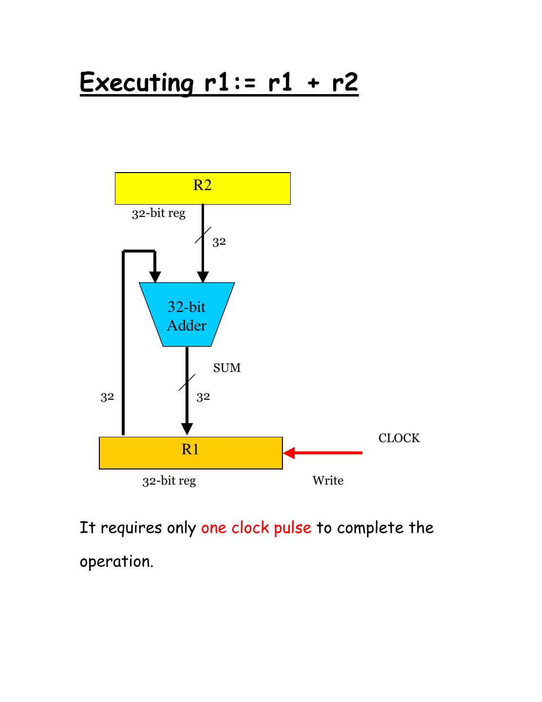
10 .Executing r1:= r1 + r2 R2 32-bit reg 32 32-bit Adder SUM 32 32 CLOCK R1 32-bit reg Write It requires only one clock pulse to complete the operation.
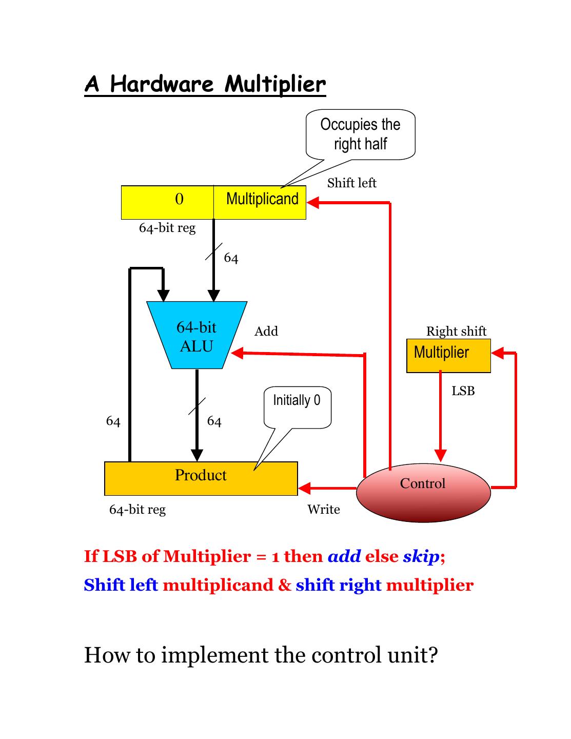
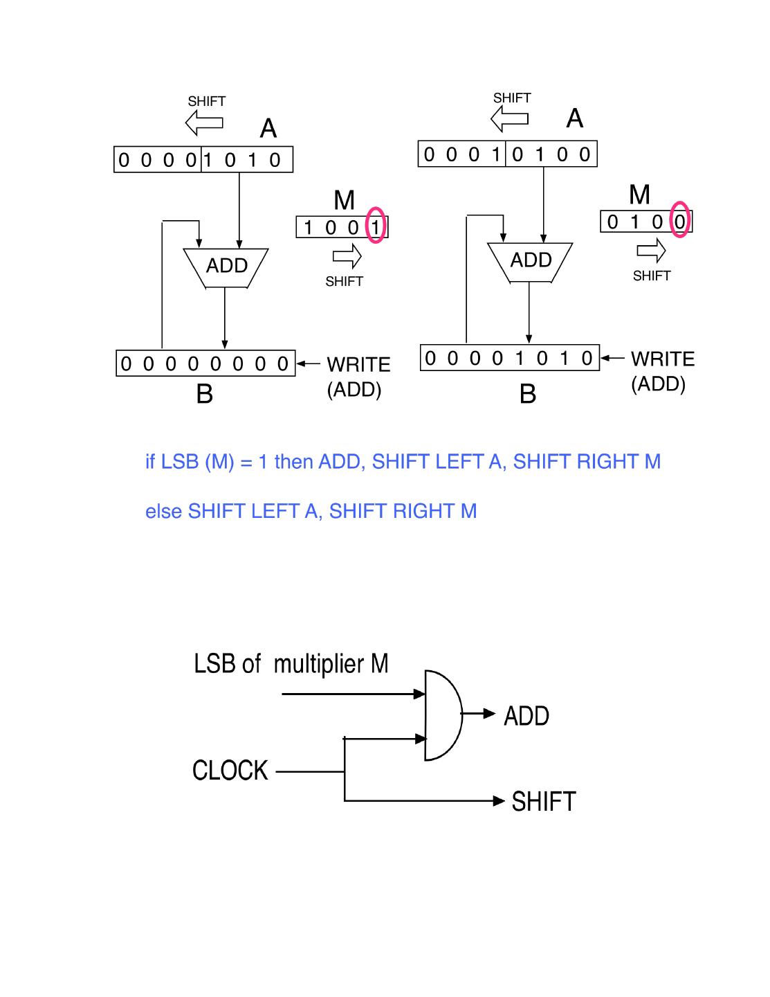
11 .A Hardware Multiplier Occupies the right half Shift left 0 Multiplicand 64-bit reg 64 64-bit Add Right shift ALU Multiplier LSB Initially 0 64 64 Product Control 64-bit reg Write If LSB of Multiplier = 1 then add else skip; Shift left multiplicand & shift right multiplier How to implement the control unit?
12 .
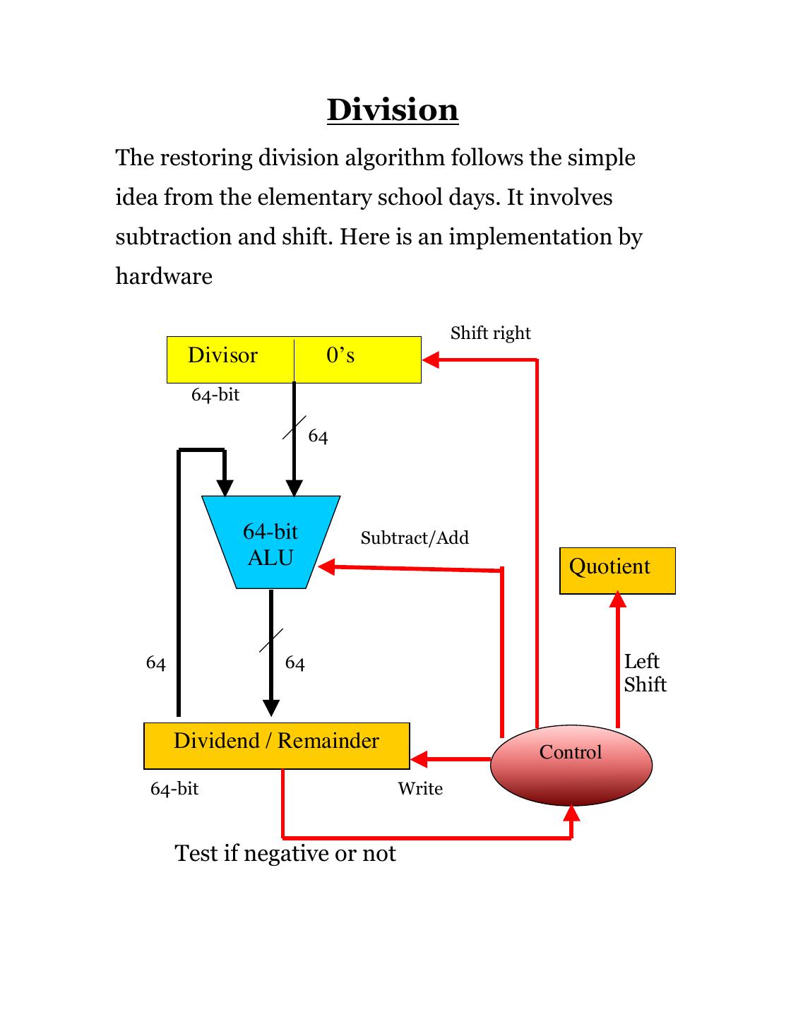
13 . Division The restoring division algorithm follows the simple idea from the elementary school days. It involves subtraction and shift. Here is an implementation by hardware Shift right Divisor 0’s 64-bit 64 64-bit Subtract/Add ALU Quotient 64 64 Left Shift Dividend / Remainder Control 64-bit Write Test if negative or not


