- 快召唤伙伴们来围观吧
- 微博 QQ QQ空间 贴吧
- 文档嵌入链接
- 复制
- 微信扫一扫分享
- 已成功复制到剪贴板
I-V特性,欧姆接触,小信号电容
展开查看详情
1 . Lecture #9 OUTLINE – Metal-semiconductor contacts (cont.) » I-V characteristics » practical ohmic contacts » small-signal capacitance Reading: Finish Chapter 14 Spring 2003 EE130 Lecture 9, Slide 1 Review: Schottky Diode (n-type Si) metal n-type Si ΦM > ΦS Eo χSi ΦM qVbi = ΦBn – (Ec – EF)FB ΦBn Ec Equilibrium (VA = 0) EF -> EF continuous, constant ΦBn = ΦM – χ Ev W Spring 2003 EE130 Lecture 9, Slide 2 1
2 . Schottky Diode (p-type Si) metal p-type Si Eo ΦM < ΦS χSi Ec ΦM Equilibrium (VA = 0) -> EF continuous, EF constant Ev ΦBp qVbi = ΦBp– (EF – Ev)FB ΦBp = χ + EG - ΦM W Spring 2003 EE130 Lecture 9, Slide 3 Depleted Layer Width, W Last time, we found that − qN D V (x ) = (W − x )2 2K Sε 0 At x = 0, V = - (Vbi - VA) 2ε s (Vbi − VA ) ⇒ W= qN D • W increases with increasing –VA • W decreases with increasing ND - (Vbi - VA) Spring 2003 EE130 Lecture 9, Slide 4 2
3 . W for p-type Semiconductor qN A V (x ) = (W − x )2 2 K Sε 0 At x = 0, V = Vbi + VA 2ε s (VA + Vbi ) ⇒ W= qN A • W increases with increasing VA • W decreases with increasing NA Spring 2003 EE130 Lecture 9, Slide 5 Current Flow in a Schottky Diode • Diode current is determined by majority- carrier flow across the MS junction – Under forward bias, majority-carrier diffusion from the semiconductor into the metal dominates the current – Under reverse bias, majority-carrier diffusion from the metal into the semiconductor dominates the current Spring 2003 EE130 Lecture 9, Slide 6 3
4 . Thermionic Emission Theory • Electrons can cross the junction if 1 mv x ≥ q(Vbi − VA ) 2 KE x = 2 2q v x ≥ vmin ≡ (Vbi − VA ) mn* • The current for electrons at a given velocity is: I s • → M , v x = − qAv x n(vx ) • So, the total current over the barrier is: − v min I s • → M = −qA ∫ v n(v )dv −∞ x x x Spring 2003 EE130 Lecture 9, Slide 7 Schottky Diode I - V • Given that 4πkTmn* 2 ( E − E ) / kT −(m* / 2 kT )v 2 n (v x ) = 3 e F c e n x h • We obtain 4πqmn k 2 I S •→ M = AT 2e − qΦ B / kT e qVA / kT h3 = AT 2 J S e qVA / kT , where J S ≈ 120e −qΦ B / kT A/cm 2 • In the other direction, we always see the same barrier ΦBn: I M • → S = − I S • → M (VA = 0) • Therefore I = I S ( e − 1) where I S = AT 2 J S qV A / kT Spring 2003 EE130 Lecture 9, Slide 8 4
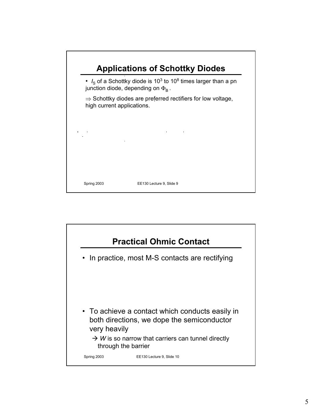
5 . Applications of Schottky Diodes • IS of a Schottky diode is 103 to 108 times larger than a pn junction diode, depending on ΦB . ⇒ Schottky diodes are preferred rectifiers for low voltage, high current applications. Spring 2003 EE130 Lecture 9, Slide 9 Practical Ohmic Contact • In practice, most M-S contacts are rectifying • To achieve a contact which conducts easily in both directions, we dope the semiconductor very heavily Æ W is so narrow that carriers can tunnel directly through the barrier Spring 2003 EE130 Lecture 9, Slide 10 5
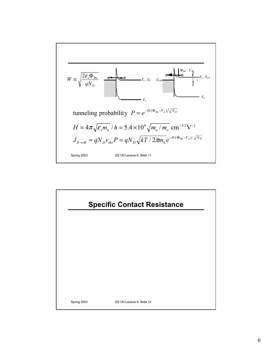
6 . ΦBn – VA 2ε s Φ Bn - - - - Ec , EFS W ≅ Ec , EF EFM V qN D Ev Ev − H ( Φ Bn −V A ) ND tunneling probabilit y P = e H = 4π ε s mn / h = 5.4 × 10⁹ mn / mo cm −3/2 V −1 − H ( Φ Bn −V A ) / N D J S → M ≈ qN D vthx P = qN D kT / 2πmn e Spring 2003 EE130 Lecture 9, Slide 11 Specific Contact Resistance Spring 2003 EE130 Lecture 9, Slide 12 6
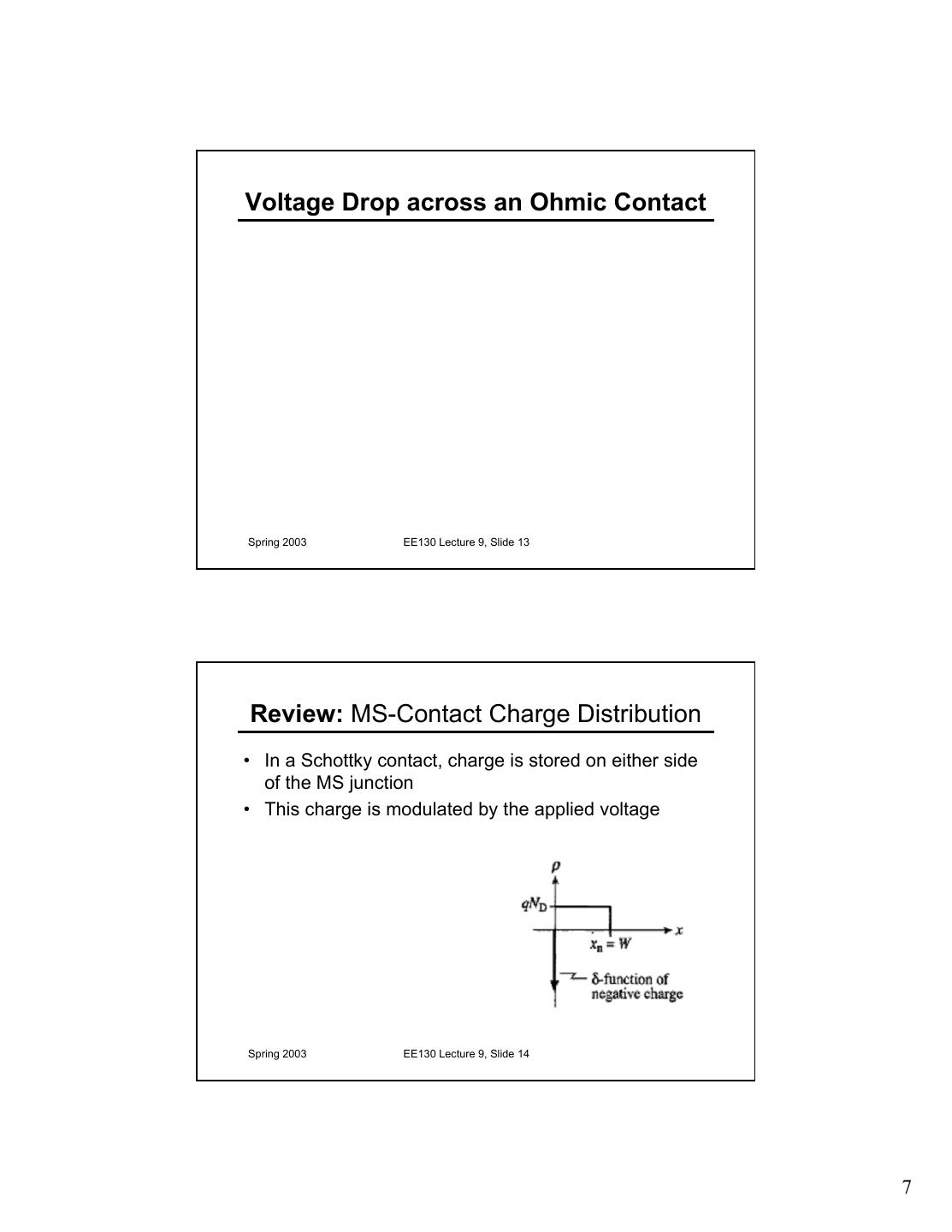
7 .Voltage Drop across an Ohmic Contact Spring 2003 EE130 Lecture 9, Slide 13 Review: MS-Contact Charge Distribution • In a Schottky contact, charge is stored on either side of the MS junction • This charge is modulated by the applied voltage Spring 2003 EE130 Lecture 9, Slide 14 7
8 .Schottky Diode: Small-Signal Capacitance • If an A.C. voltage is applied in series with the D.C. bias VA, the charge stored in the Schottky contact will be modulated → displacement current will flow εs C= A W Spring 2003 EE130 Lecture 9, Slide 15 Using C-V Data to Determine ΦB 1 2(Vbi − VA ) = C 2 qN Dε s A2 Once Vbi is known, ΦΒn can be determined: Nc qVbi = qΦ Bn − ( Ec − EF ) FB = qΦ Bn − kT ln ND Spring 2003 EE130 Lecture 9, Slide 16 8
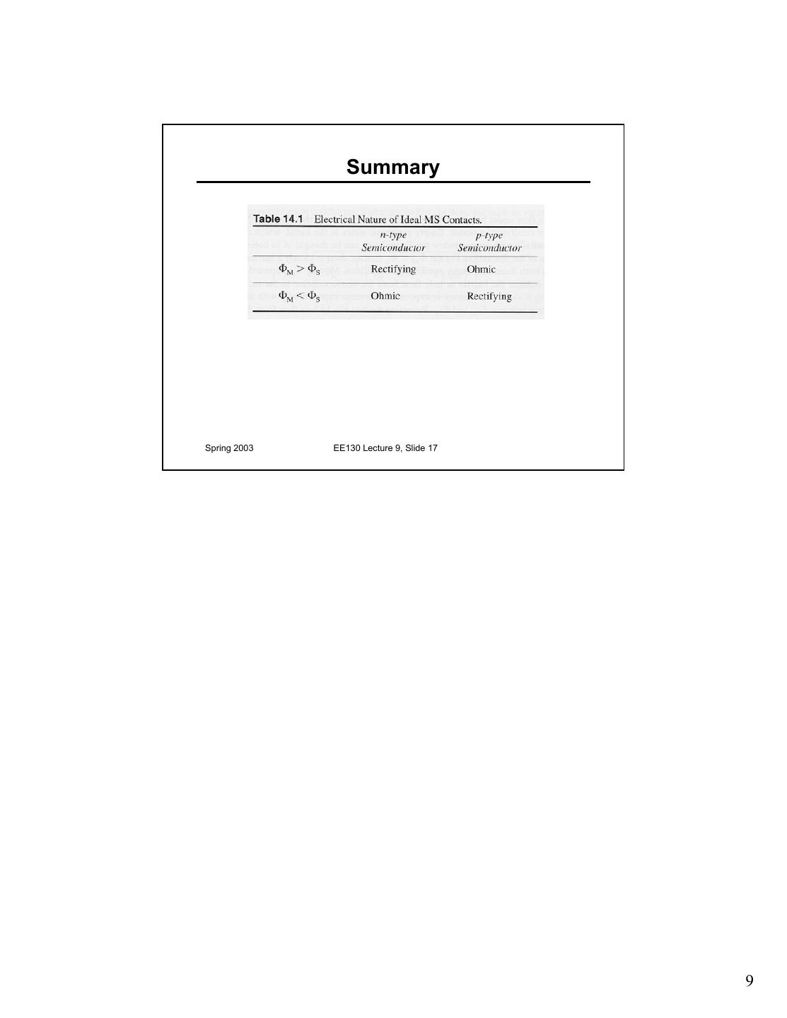
9 . Summary Spring 2003 EE130 Lecture 9, Slide 17 9


