- 快召唤伙伴们来围观吧
- 微博 QQ QQ空间 贴吧
- 文档嵌入链接
- 复制
- 微信扫一扫分享
- 已成功复制到剪贴板
集成电路器件
展开查看详情
1 . EE130: Integrated Circuit Devices (online at http://webcast.berkeley.edu) Instructor: Prof. Tsu-Jae King (tking@eecs.berkeley.edu) TA’s: Marie Eyoum (meyoum@eecs.berkeley.edu) Alvaro Padilla (apadilla@eecs.berkeley.edu) Web page: http://www-inst.eecs.berkeley.edu/~ee130/ Newsgroup: ucb.class.ee130 Course Outline 1. Semiconductor Fundamentals – 3 weeks 2. Metal-Semiconductor Contacts – 1 week 3. P-N Junction Diode – 3 weeks 4. Bipolar Junction Transistor – 3 weeks 5. MOS Capacitor – 1 week 6. MOSFET – 4 weeks Gate Source Drain Substrate Spring 2003 1
2 . Introduction Integrated-Circuit Devices Power4 µP 4004 µP Spring 2003 2
3 . Planar Process Technology *planar starting multiple devices + processing = monolithically integrated substrate steps Si wafer n-channel MOSFET *sequence of additive and subtractive steps with lateral patterning oxidation etching lithography deposition ion implantation Spring 2003 IC Technology Advancement Rapid advances in IC technology have been achieved primarily by scaling down transistor lateral dimensions Technology Scaling 100 ITRS 2001 Projection Investment Better Performance/Cost GATE LENGTH (nm) Market Growth 10 LOW POWER HIGH PERFORMANCE 1 2000 2005 2010 2015 2020 YEAR Spring 2003 3
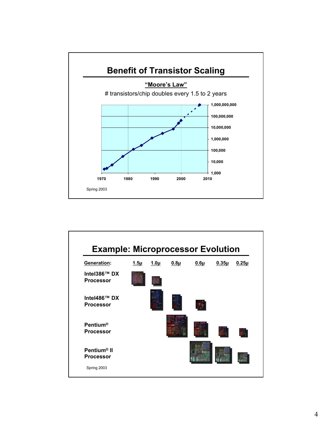
4 . Benefit of Transistor Scaling “Moore’s Law” # transistors/chip doubles every 1.5 to 2 years 1,000,000,000 100,000,000 10,000,000 1,000,000 100,000 10,000 1,000 1970 1980 1990 2000 2010 Spring 2003 Example: Microprocessor Evolution Generation: 1.5µ 1.0µ 0.8µ 0.6µ 0.35µ 0.25µ Intel386™ DX Processor Intel486™ DX Processor Pentium® Processor Pentium® II Processor Spring 2003 4
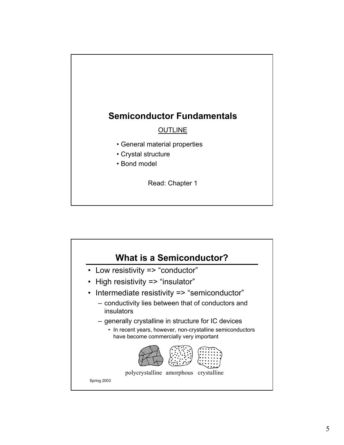
5 . Semiconductor Fundamentals OUTLINE • General material properties • Crystal structure • Bond model Read: Chapter 1 What is a Semiconductor? • Low resistivity => “conductor” • High resistivity => “insulator” • Intermediate resistivity => “semiconductor” – conductivity lies between that of conductors and insulators – generally crystalline in structure for IC devices • In recent years, however, non-crystalline semiconductors have become commercially very important polycrystalline amorphous crystalline Spring 2003 5
6 . Semiconductor Materials Elemental: Compound: Alloy: Spring 2003 From Hydrogen to Silicon # of Electrons 1 2 3 Z Name 1s 2s 2p 3s 3p 3d Notation 1H 1 1s 1 2 He 2 1s 2 3 Li 2 1 1s 2 2s 1 4 Be 2 2 1s 2 2s 2 5B 2 2 1 1s 2 2s 2 2p1 6C 2 2 2 1s 2 2s 2 2p2 7N 2 2 3 1s 2 2s 2 2p3 8O 2 2 4 1s 2 2s 2 2p4 9F 2 2 5 1s 2 2s 2 2p5 10 Ne 2 2 6 1s 2 2s 2 2p6 11 Na 2 2 6 1 1s 2 2s 2 2p6 3s 1 12 Mg 2 2 6 2 1s 2 2s 2 2p6 3s 2 13 Al 2 2 6 2 1 1s 2 2s 2 2p6 3s 2 3p1 14 Si 2 2 6 2 2 1s 2 2s 2 2p6 3s 2 3p2 15 P 2 2 6 2 3 1s 2 2s 2 2p6 3s 2 3p3 16 S 2 2 6 2 4 1s 2 2s 2 2p6 3s 2 3p4 17 Cl 2 2 6 2 5 1s 2 2s 2 2p6 3s 2 3p5 18 Ar 2 2 6 2 6 1s 2 2s 2 2p6 3s 2 3p6 Spring 2003 6
7 . The Silicon Atom • 14 electrons occupying the 1st 3 energy levels: – 1s, 2s, 2p orbitals filled by 10 electrons – 3s, 3p orbitals filled by 4 electrons To minimize the overall energy, the 3s and 3p orbitals hybridize to form 4 tetrahedral 3sp orbitals Each has one electron and is capable of forming a bond with a neighboring atom Spring 2003 The Si Crystal • Each Si atom has 4 nearest neighbors • lattice constant = 5.431Å “diamond cubic” lattice Spring 2003 7
8 . Compound Semiconductors Ga As • “zincblende” structure • III-V compound semiconductors: GaAs, GaP, GaN, etc. 9 important for optoelectronics and high-speed ICs Spring 2003 Crystallographic Notation Miller Indices: Notation Interpretation (hkl) crystal plane {hkl} equivalent planes [hkl] crystal direction <hkl> equivalent directions h: inverse x-intercept of plane k: inverse y-intercept of plane l: inverse z-intercept of plane (Intercept values are in multiples of the lattice constant; h, k and l are reduced to 3 integers having the same ratio.) Spring 2003 8
9 . Crystallographic Planes and Si Wafers Silicon wafers are usually cut along the (100) plane with a (100) plane flat or notch to orient the (011) wafer during IC fabrication: flat Spring 2003 Crystallographic Planes in Si Unit cell: lattice constant = 5.431Å Æ 5 x 10²² atoms/cm3 View in <111> direction View in <100> direction View in <110> direction Spring 2003 9
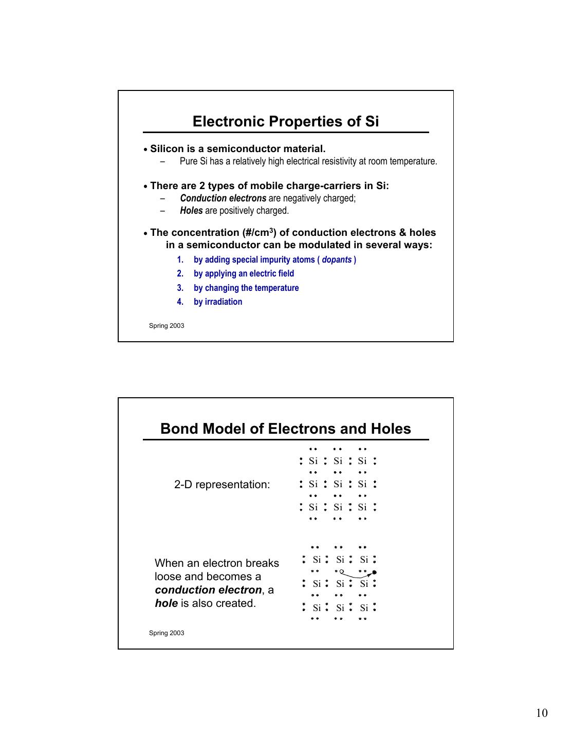
10 . Electronic Properties of Si • Silicon is a semiconductor material. – Pure Si has a relatively high electrical resistivity at room temperature. • There are 2 types of mobile charge-carriers in Si: – Conduction electrons are negatively charged; – Holes are positively charged. • The concentration (#/cm3) of conduction electrons & holes in a semiconductor can be modulated in several ways: 1. by adding special impurity atoms ( dopants ) 2. by applying an electric field 3. by changing the temperature 4. by irradiation Spring 2003 Bond Model of Electrons and Holes Si Si Si 2-D representation: Si Si Si Si Si Si When an electron breaks Si Si Si loose and becomes a Si Si Si conduction electron, a hole is also created. Si Si Si Spring 2003 10
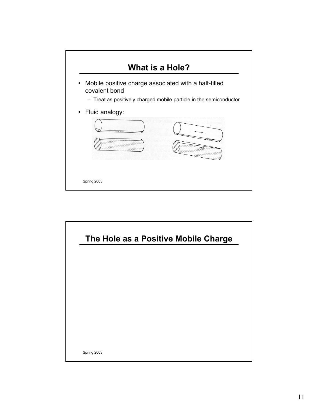
11 . What is a Hole? • Mobile positive charge associated with a half-filled covalent bond – Treat as positively charged mobile particle in the semiconductor • Fluid analogy: Spring 2003 The Hole as a Positive Mobile Charge Spring 2003 11
12 . Pure Si conduction ni ≅ 1010 cm-3 at room temperature Spring 2003 Summary • Crystalline Si: – 4 valence electrons per atom – diamond lattice: each atom has 4 nearest neighbors – 5 x 10²² atoms/cm3 • In a pure Si crystal, conduction electrons and holes are formed in pairs. – Holes can be considered as positively charged mobile particles which exist inside a semiconductor. – Both holes and electrons can conduct current. Spring 2003 12


