- 快召唤伙伴们来围观吧
- 微博 QQ QQ空间 贴吧
- 文档嵌入链接
- 复制
- 微信扫一扫分享
- 已成功复制到剪贴板
能带模型及其发展
展开查看详情
1 . Lecture #2 OUTLINE • Energy-band model • Doping Read: Chapter 2 Definition of Terms n = number of electrons/cm3 p = number of holes/cm3 ni = intrinsic carrier concentration In a pure semiconductor, n = p = ni Spring 2003 EE130 Lecture 2, Slide 2 1
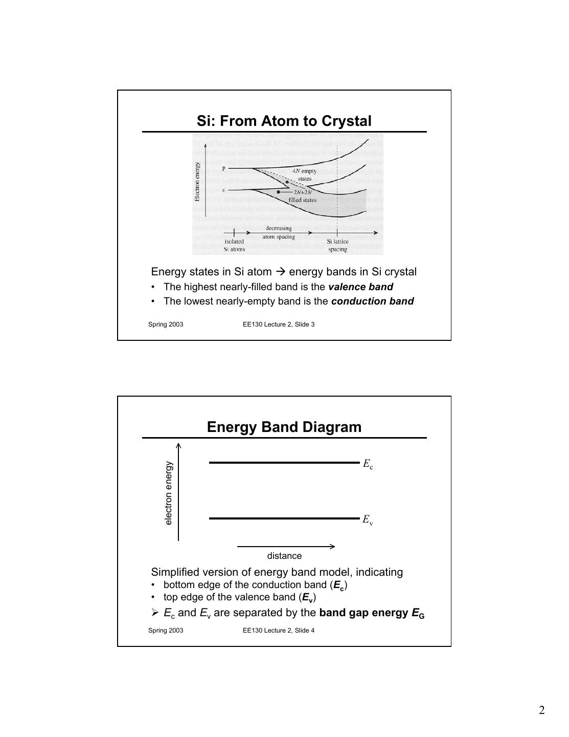
2 . Si: From Atom to Crystal Energy states in Si atom Æ energy bands in Si crystal • The highest nearly-filled band is the valence band • The lowest nearly-empty band is the conduction band Spring 2003 EE130 Lecture 2, Slide 3 Energy Band Diagram Ec electron energy Ev distance Simplified version of energy band model, indicating • bottom edge of the conduction band (Ec) • top edge of the valence band (Ev) ¾ Ec and Ev are separated by the band gap energy EG Spring 2003 EE130 Lecture 2, Slide 4 2
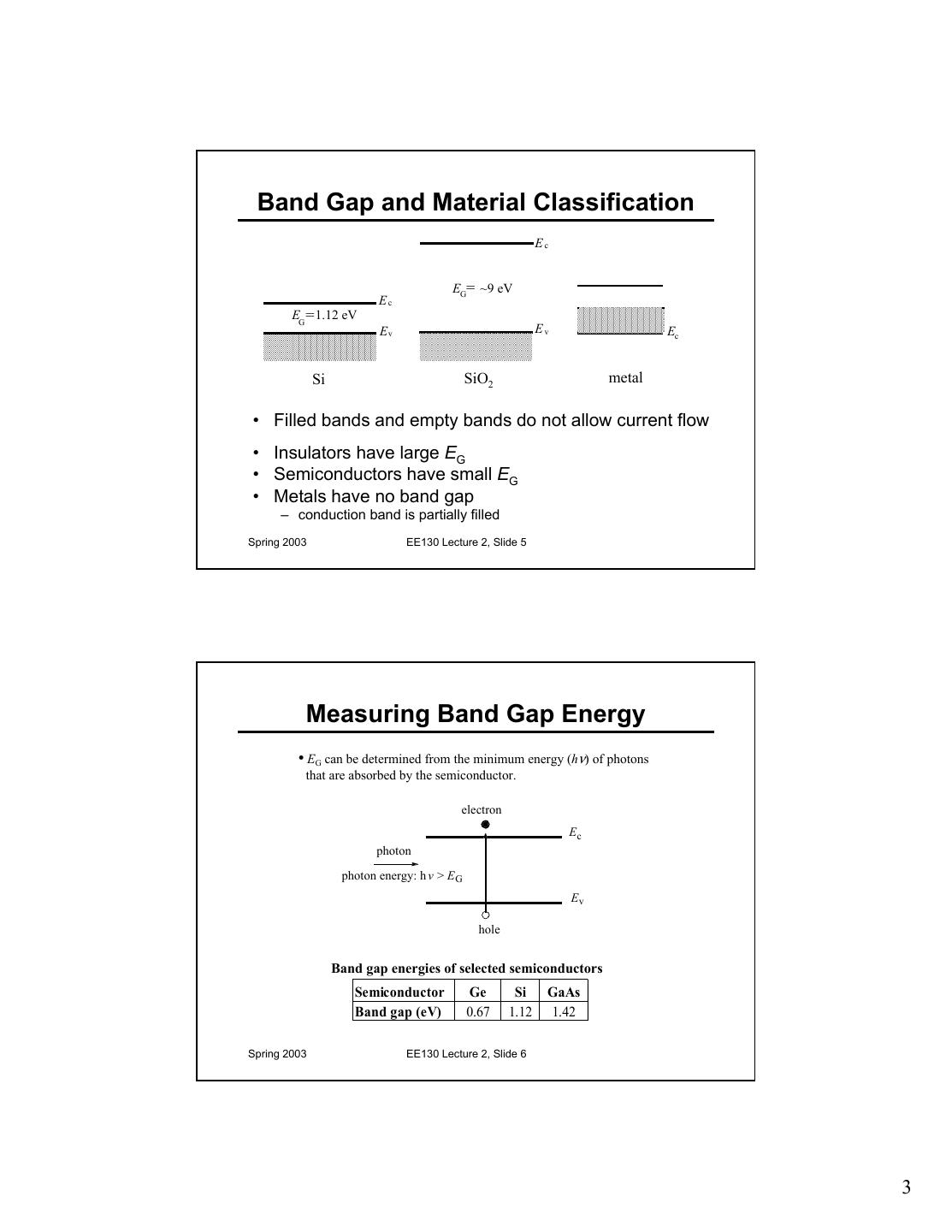
3 . Band Gap and Material Classification Ec EG= ~9 eV Ec EG = 1.12 eV Ev Ev Ec Si SiO2 metal • Filled bands and empty bands do not allow current flow • Insulators have large EG • Semiconductors have small EG • Metals have no band gap – conduction band is partially filled Spring 2003 EE130 Lecture 2, Slide 5 Measuring Band Gap Energy • EG can be determined from the minimum energy (hν) of photons that are absorbed by the semiconductor. electron Ec photon photon energy: h v > E G Ev hole Band gap energies of selected semiconductors Semiconductor Ge Si GaAs Band gap (eV) 0.67 1.12 1.42 Spring 2003 EE130 Lecture 2, Slide 6 3
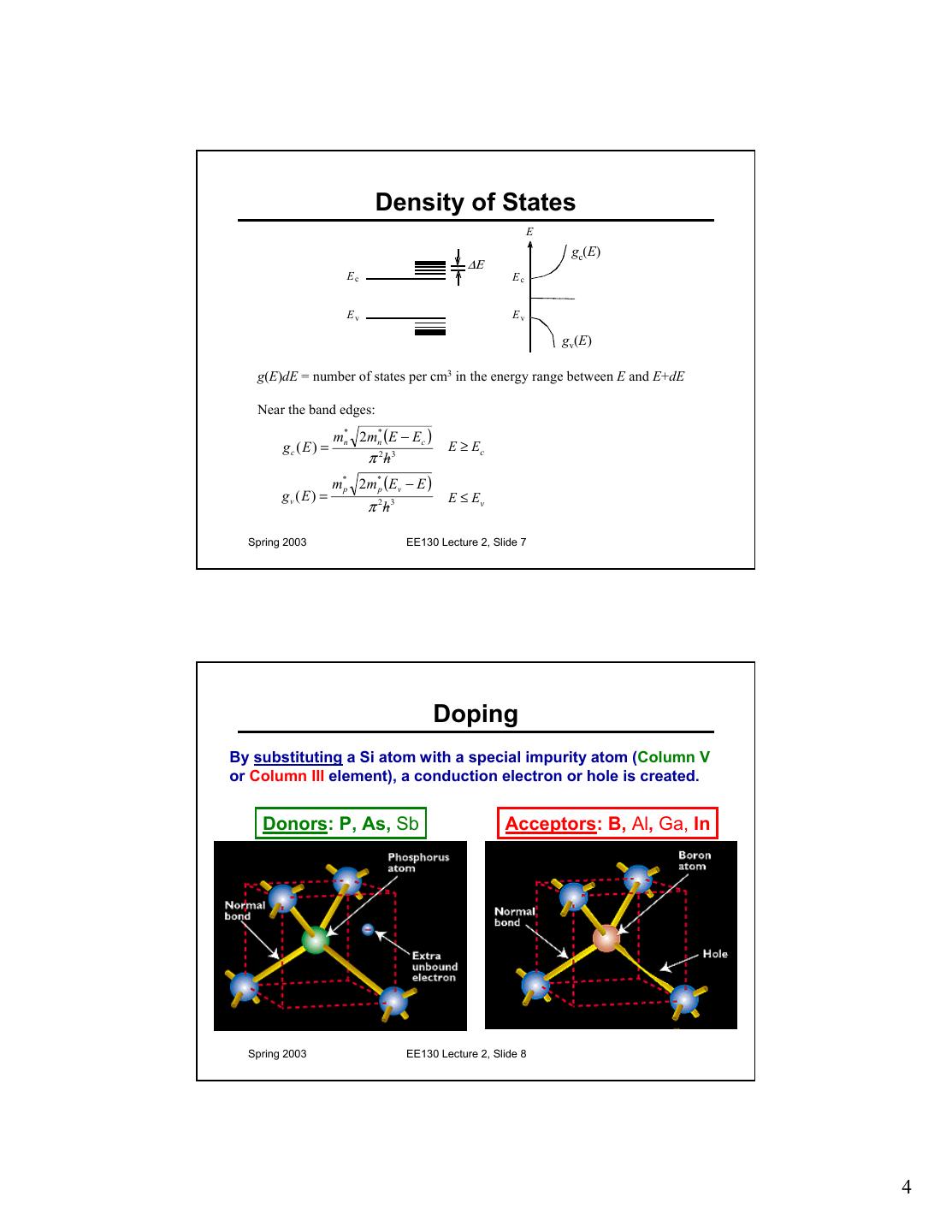
4 . Density of States E gc(E) ∆Ε Ec Ec Ev Ev gv(E) g(E)dE = number of states per cm3 in the energy range between E and E+dE Near the band edges: mn* 2mn* (E − Ec ) gc ( E ) = E ≥ Ec π 2h 3 m*p 2m*p (Ev − E ) gv ( E ) = E ≤ Ev π 2h 3 Spring 2003 EE130 Lecture 2, Slide 7 Doping By substituting a Si atom with a special impurity atom (Column V or Column III element), a conduction electron or hole is created. Donors: P, As, Sb Acceptors: B, Al, Ga, In Spring 2003 EE130 Lecture 2, Slide 8 4
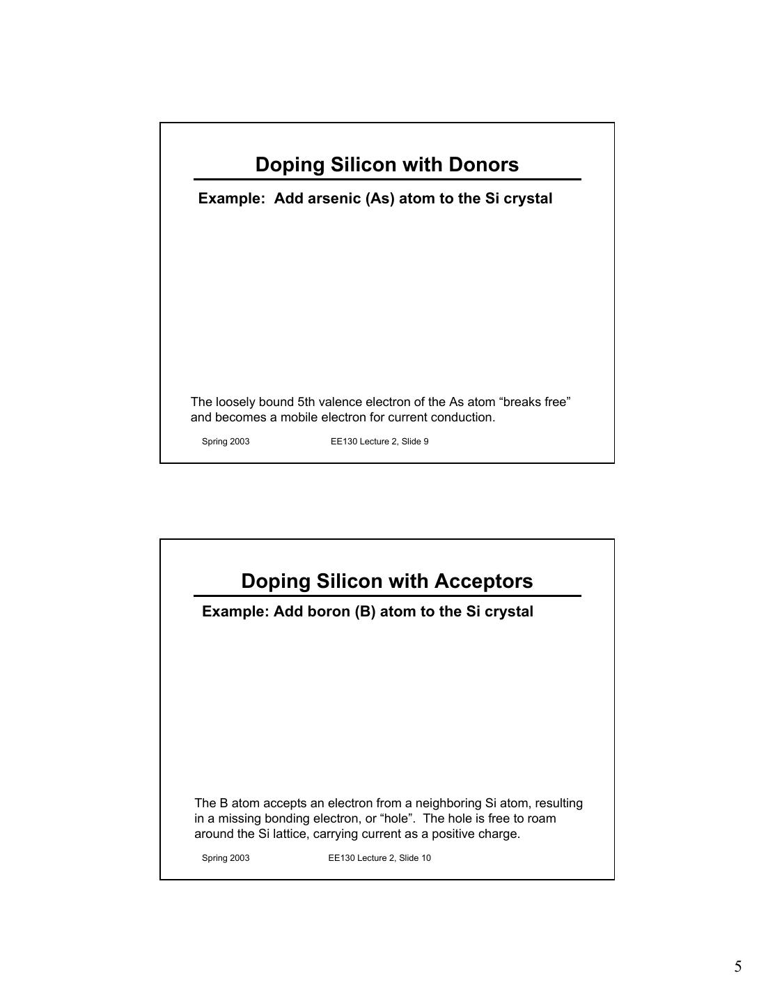
5 . Doping Silicon with Donors Example: Add arsenic (As) atom to the Si crystal The loosely bound 5th valence electron of the As atom “breaks free” and becomes a mobile electron for current conduction. Spring 2003 EE130 Lecture 2, Slide 9 Doping Silicon with Acceptors Example: Add boron (B) atom to the Si crystal The B atom accepts an electron from a neighboring Si atom, resulting in a missing bonding electron, or “hole”. The hole is free to roam around the Si lattice, carrying current as a positive charge. Spring 2003 EE130 Lecture 2, Slide 10 5
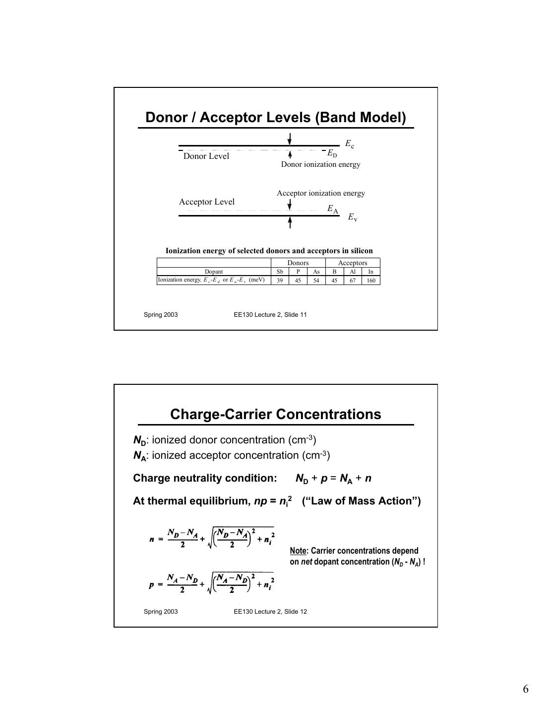
6 . Donor / Acceptor Levels (Band Model) Ec Donor Level ED Donor ionization energy Acceptor ionization energy Acceptor Level EA Ev Ionization energy of selected donors and acceptors in silicon Donors Acceptors Dopant Sb P As B Al In Ionization energy, E c -E d or E a -E v (meV) 39 45 54 45 67 160 Spring 2003 EE130 Lecture 2, Slide 11 Charge-Carrier Concentrations ND: ionized donor concentration (cm-3) NA: ionized acceptor concentration (cm-3) Charge neutrality condition: ND + p = NA + n At thermal equilibrium, np = ni2 (“Law of Mass Action”) Note: Carrier concentrations depend on net dopant concentration (ND - NA) ! Spring 2003 EE130 Lecture 2, Slide 12 6
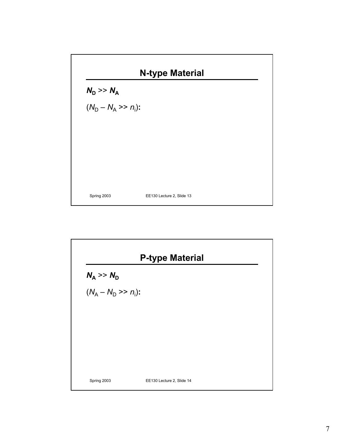
7 . N-type Material ND >> NA (ND – NA >> ni): Spring 2003 EE130 Lecture 2, Slide 13 P-type Material NA >> ND (NA – ND >> ni): Spring 2003 EE130 Lecture 2, Slide 14 7
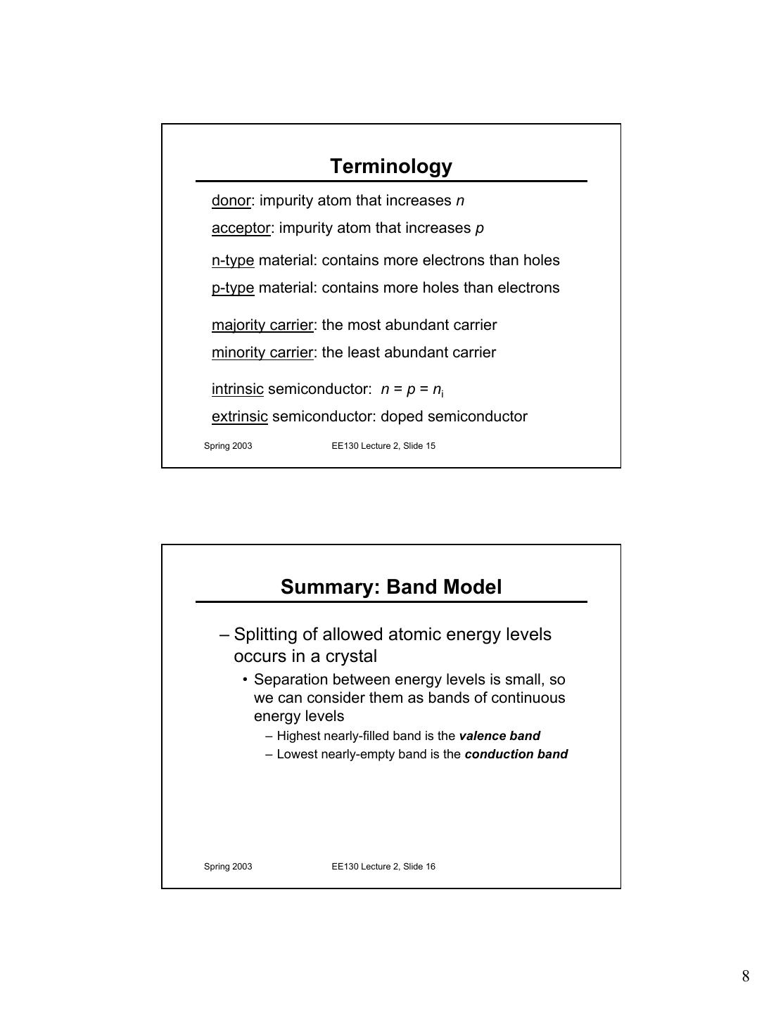
8 . Terminology donor: impurity atom that increases n acceptor: impurity atom that increases p n-type material: contains more electrons than holes p-type material: contains more holes than electrons majority carrier: the most abundant carrier minority carrier: the least abundant carrier intrinsic semiconductor: n = p = ni extrinsic semiconductor: doped semiconductor Spring 2003 EE130 Lecture 2, Slide 15 Summary: Band Model – Splitting of allowed atomic energy levels occurs in a crystal • Separation between energy levels is small, so we can consider them as bands of continuous energy levels – Highest nearly-filled band is the valence band – Lowest nearly-empty band is the conduction band Spring 2003 EE130 Lecture 2, Slide 16 8
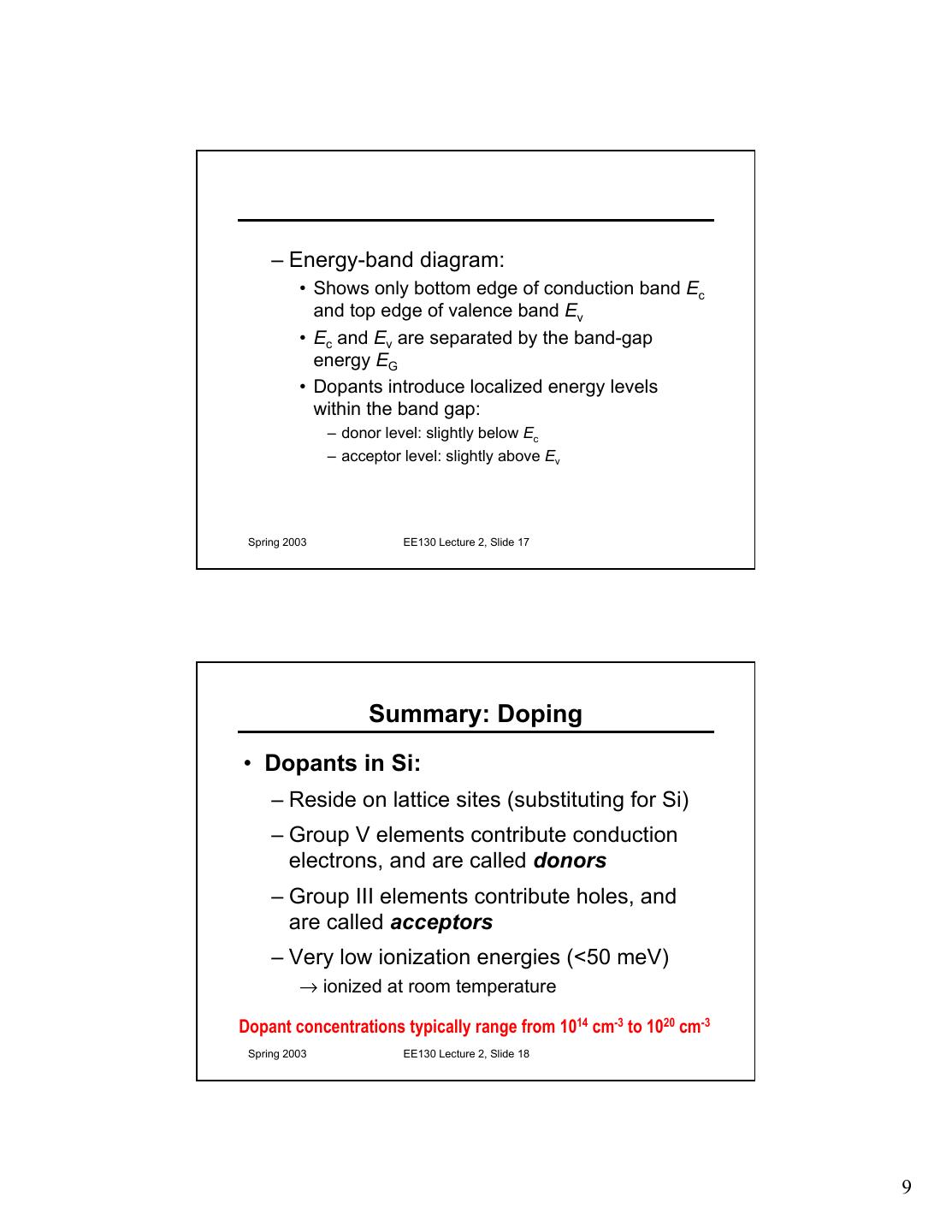
9 . – Energy-band diagram: • Shows only bottom edge of conduction band Ec and top edge of valence band Ev • Ec and Ev are separated by the band-gap energy EG • Dopants introduce localized energy levels within the band gap: – donor level: slightly below Ec – acceptor level: slightly above Ev Spring 2003 EE130 Lecture 2, Slide 17 Summary: Doping • Dopants in Si: – Reside on lattice sites (substituting for Si) – Group V elements contribute conduction electrons, and are called donors – Group III elements contribute holes, and are called acceptors – Very low ionization energies (<50 meV) → ionized at room temperature Dopant concentrations typically range from 1014 cm-3 to 1020 cm-3 Spring 2003 EE130 Lecture 2, Slide 18 9


