- 快召唤伙伴们来围观吧
- 微博 QQ QQ空间 贴吧
- 文档嵌入链接
- 复制
- 微信扫一扫分享
- 已成功复制到剪贴板
超低功率电压设计
展开查看详情
1 .Ultra-Low Power/Voltage Design
2 .Chapter Outline Rationale Lower Bounds on Computational Energy Subthreshold Logic Moderate Inversion as a Trade-off Revisiting Logic Gate Topologies Summary
3 .Rationale Continued increase of computational density must be combined with decrease in energy/operation (EOP). Further scaling of supply voltage essential to accomplish that The only other option is to keep on reducing activity Some key questions: How far can the supply voltage be scaled? What is the minimum energy per operation that can be obtained theoretically and practically? What to do about the threshold voltage and leakage? How to practically design circuits that approach the minimum energy bounds?
4 .Opportunities for Ultra-Low Voltage Number of applications emerging that do not need high performance, only extremely low power dissipation Examples: Standby operation for mobile components Implanted electronics and artificial senses Smart objects, fabrics and e-textiles Need power levels below 1 mW (even m W in certain cases)
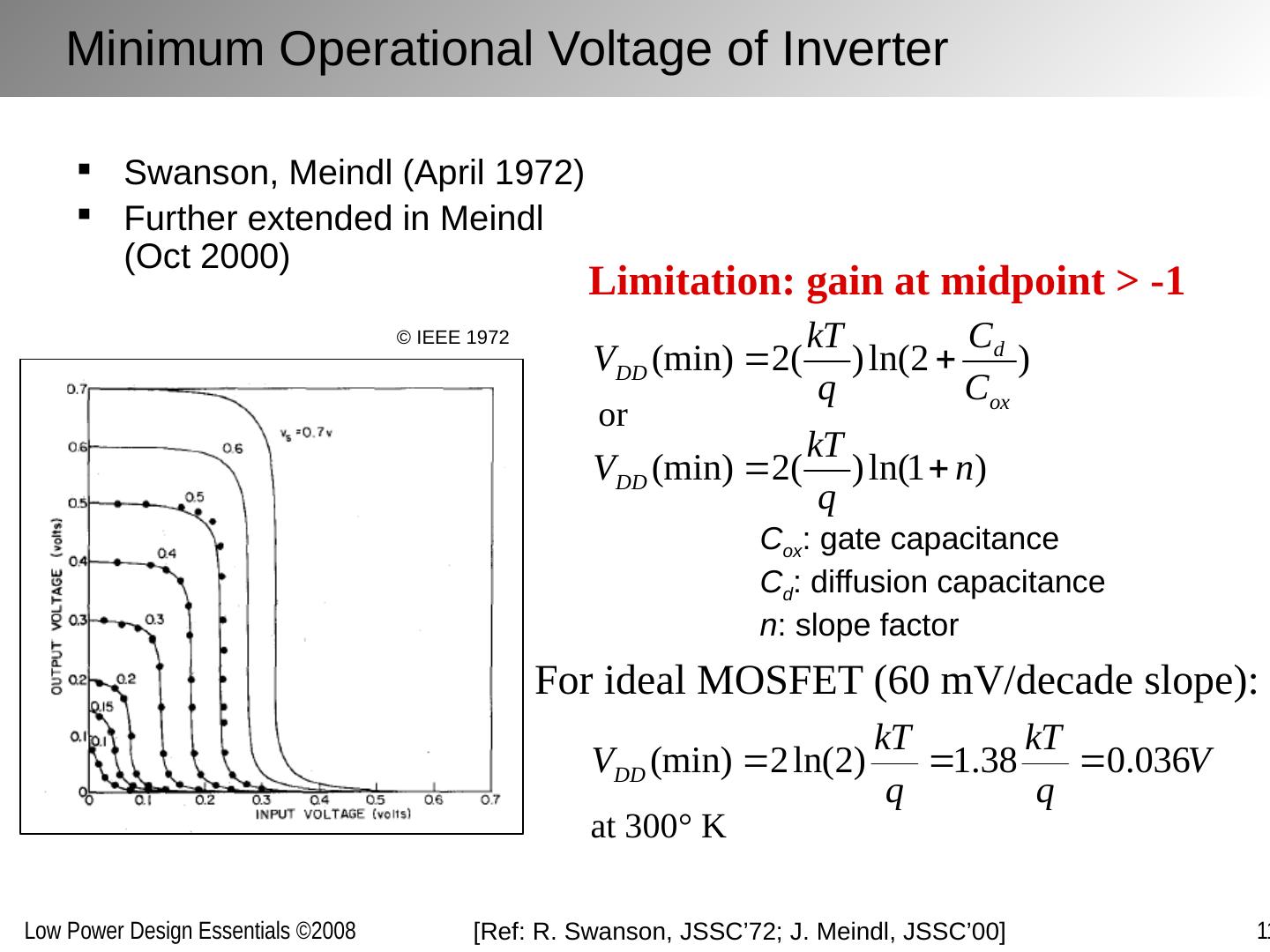
5 .Minimum Operational Voltage of Inverter Swanson, Meindl (April 1972) Further extended in Meindl (Oct 2000) Limitation: gain at midpoint > -1 C ox : gate capacitance C d : diffusion capacitance n : slope factor For ideal MOSFET (60 mV/decade slope): at 300 ° K or [ Ref: R. Swanson, JSSC’72; J. Meindl , JSSC’00] © IEEE 1972
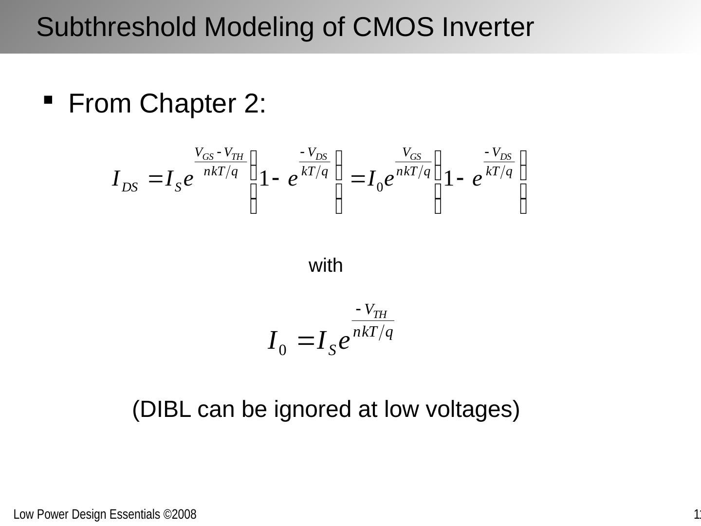
6 .Subthreshold Modeling of CMOS Inverter From Chapter 2: (DIBL can be ignored at low voltages) with
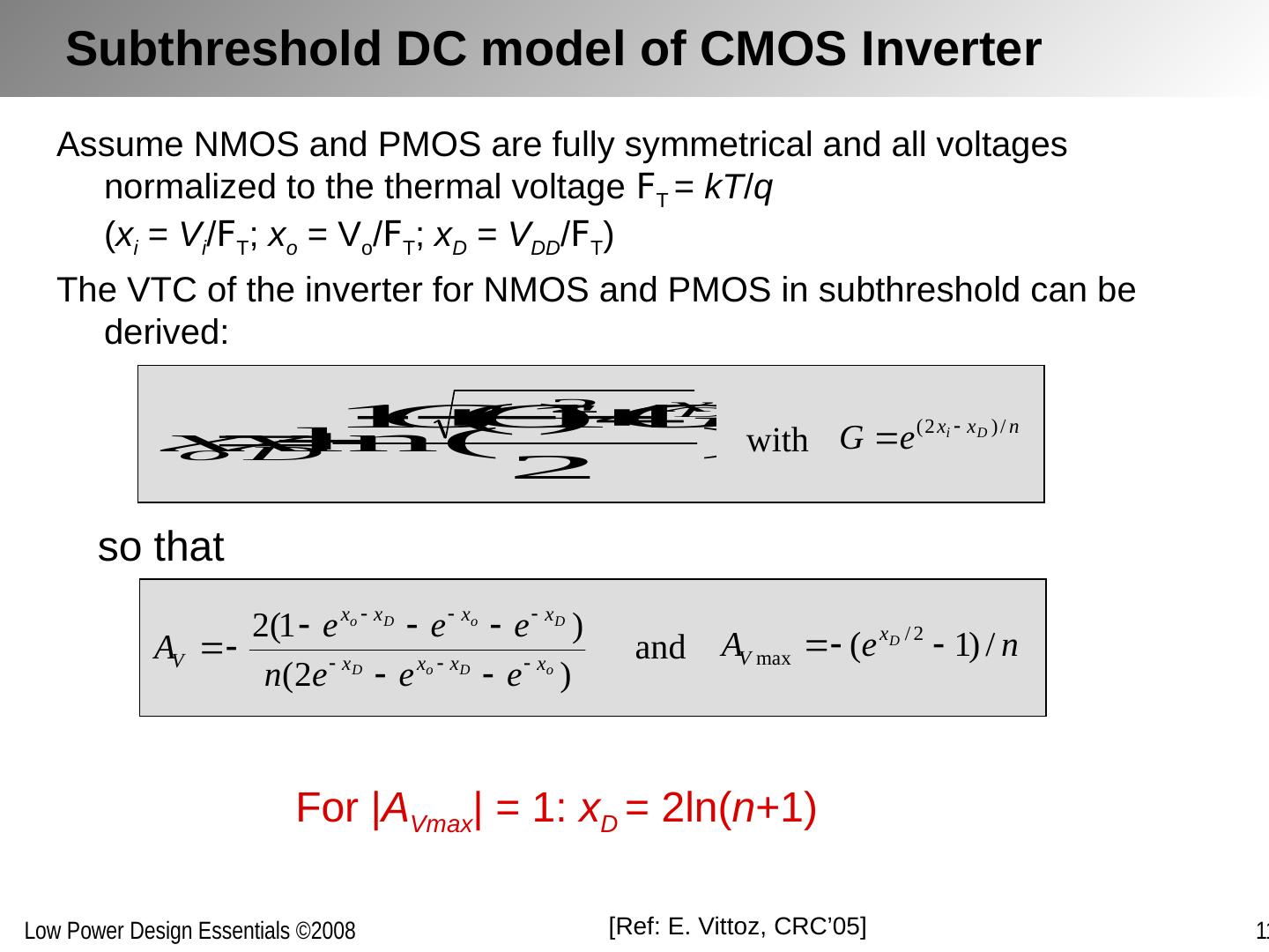
7 .Subthreshold DC model of CMOS Inverter Assume NMOS and PMOS are fully symmetrical and all voltages normalized to the thermal voltage F T = kT / q ( x i = V i / F T ; x o = V o / F T ; x D = V DD / F T ) The VTC of the inverter for NMOS and PMOS in subthreshold can be derived: [ Ref: E. Vittoz , CRC’05 ] with so that and For | A Vmax | = 1: x D = 2ln( n +1)
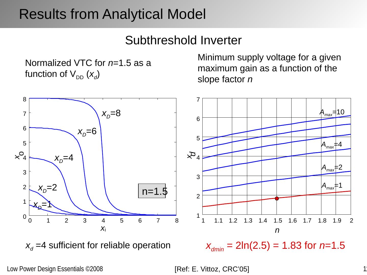
8 .Results from Analytical Model 1 1.1 1.2 1.3 1.4 1.5 1.6 1.7 1.8 1.9 2 1 2 3 4 5 6 7 n x d A max =1 A max =2 A max =4 A max =10 Normalized VTC for n =1.5 as a function of V DD ( x d ) Subthreshold Inverter Minimum supply voltage for a given maximum gain as a function of the slope factor n [ Ref: E. Vittoz , CRC’05 ] x dmin = 2ln(2.5) = 1.83 for n =1.5 x d =4 sufficient for reliable operation x D =8 x D =6 x D =4 x D =1 x D =2 n=1.5 0 1 2 3 4 5 6 7 8 0 1 2 3 4 5 6 7 8 x i x o
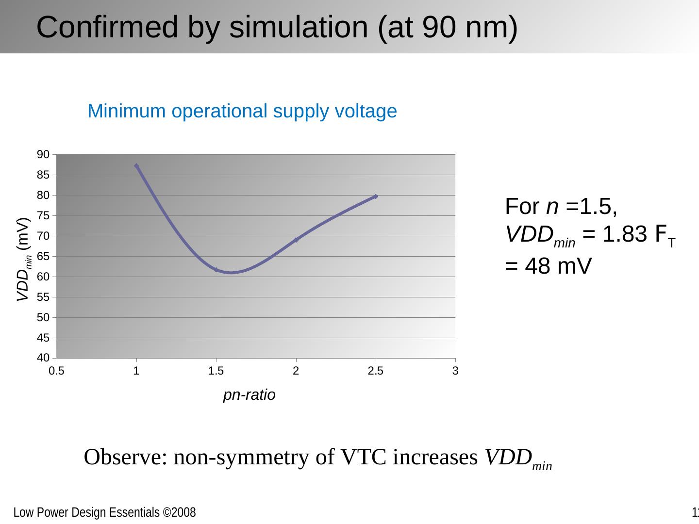
9 .Confirmed by simulation (at 90 nm) Observe: non-symmetry of VTC increases VDD min For n =1.5, VDD min = 1.83 F T = 48 mV Minimum operational supply voltage pn -ratio VDD min (mV)
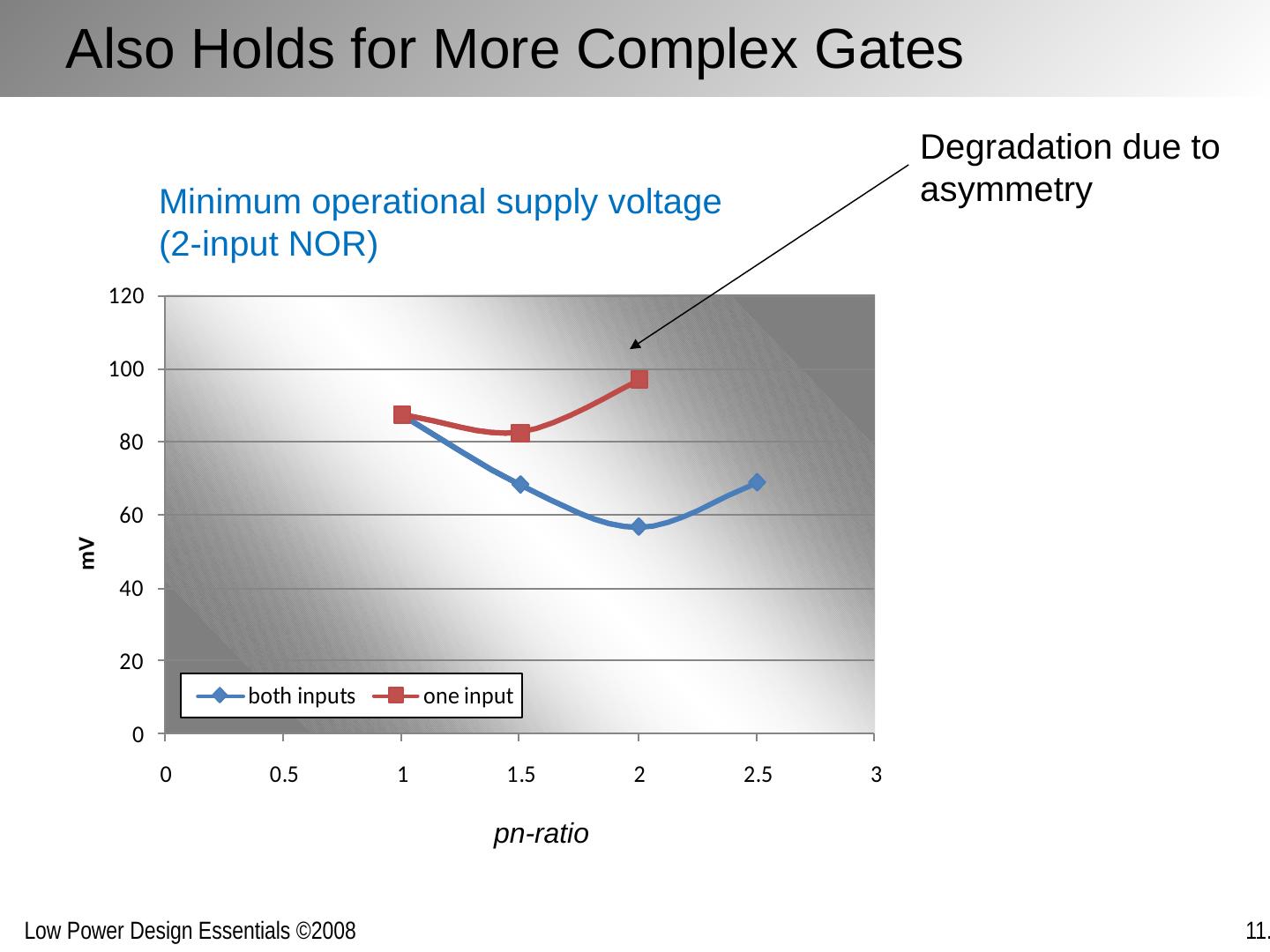
10 .Also Holds for More Complex Gates Degradation due to asymmetry Minimum operational supply voltage (2-input NOR) pn -ratio
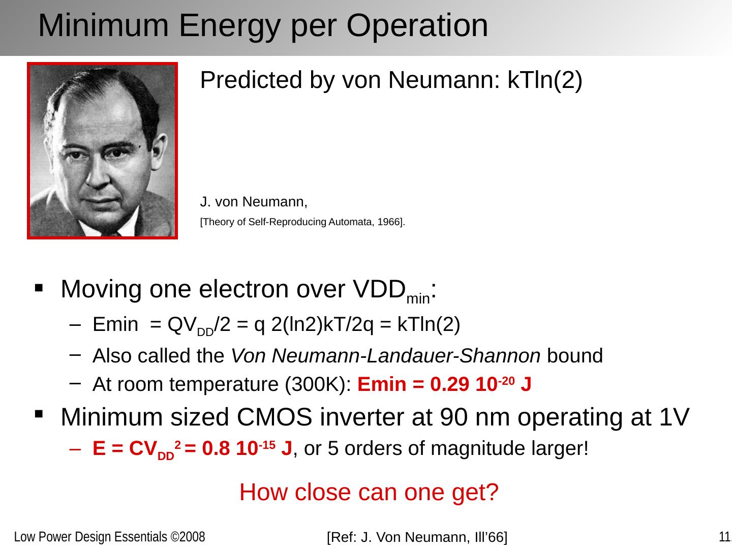
11 .Minimum Energy per Operation Moving one electron over VDD min : Emin = QV DD /2 = q 2(ln2)kT/2q = kTln(2 ) Also called the Von Neumann- Landauer -Shannon bound At room temperature (300K): Emin = 0.29 10 -20 J Minimum sized CMOS inverter at 90 nm operating at 1V E = CV DD 2 = 0.8 10 -15 J , or 5 orders of magnitude larger! J. von Neumann, [Theory of Self-Reproducing Automata, 1966] . Predicted by von Neumann: kTln(2) How close can one get? [ Ref: J. Von Neumann, Ill’66]
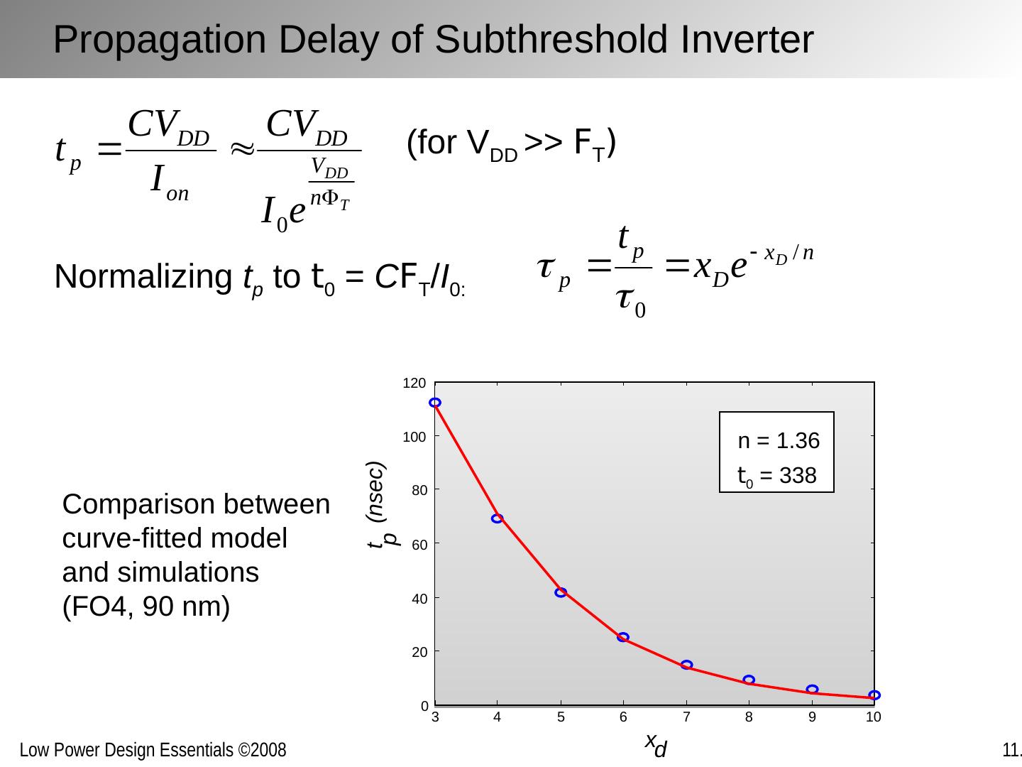
12 .Propagation Delay of Subthreshold Inverter Normalizing t p to t 0 = C F T / I 0: (for V DD >> F T ) Comparison between curve-fitted model and simulations (FO4, 90 nm) 3 4 5 6 7 8 9 10 0 20 40 60 80 100 120 x d t p t 0 = 338 n = 1.36 (nsec)
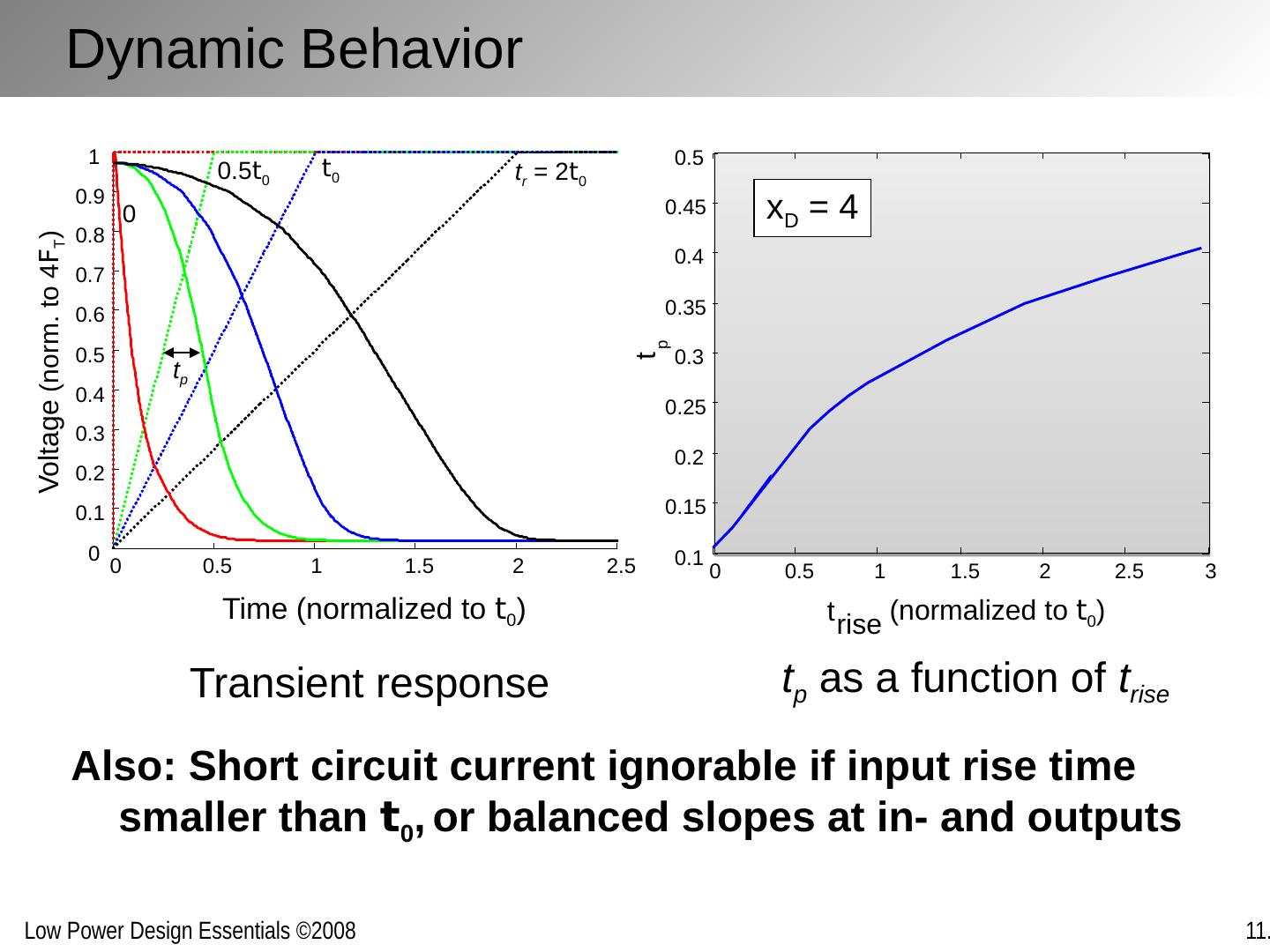
13 .Dynamic Behavior Also: Short circuit current ignorable if input rise time smaller than t 0 , or balanced slopes at in- and outputs 0 0.5 1 1.5 2 2.5 0 0.1 0.2 0.3 0.4 0.5 0.6 0.7 0.8 0.9 1 Time (normalized to t 0 ) Voltage (norm. to 4 F T ) Transient response t r = 2 t 0 t 0 0.5 t 0 0 t p t p as a function of t rise 0 0.5 1 1.5 2 2.5 3 0.1 0.15 0.2 0.25 0.3 0.35 0.4 0.45 0.5 t rise t p (normalized to t 0 ) x D = 4
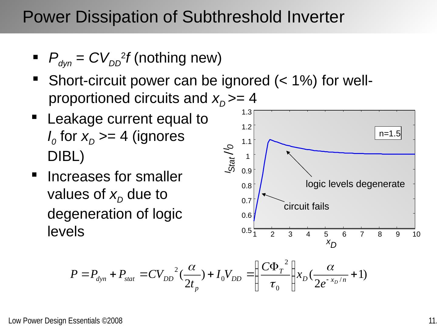
14 .Power Dissipation of Subthreshold Inverter P dyn = CV DD 2 f (nothing new) Short-circuit power can be ignored (< 1%) for well-proportioned circuits and x D >= 4 1 2 3 4 5 6 7 8 9 10 0.5 0.6 0.7 0.8 0.9 1 1.1 1.2 1.3 x D I Stat I 0 n=1.5 circuit fails logic levels degenerate Leakage current equal to I 0 for x D >= 4 (ignores DIBL) Increases for smaller values of x D due to degeneration of logic levels
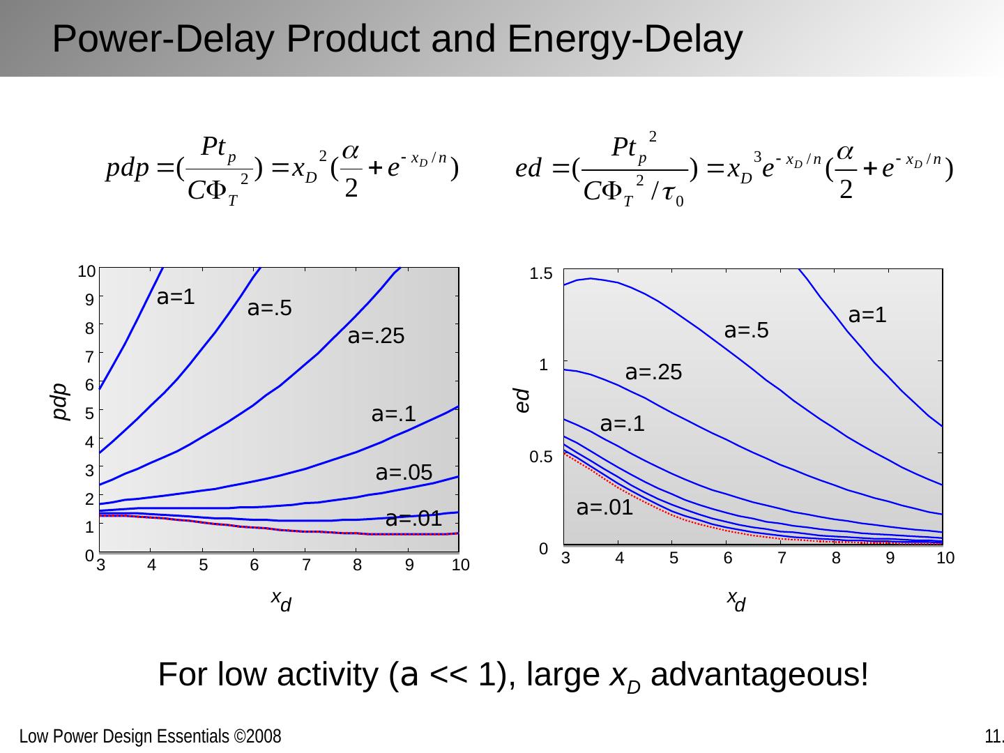
15 .Power-Delay Product and Energy-Delay 3 4 5 6 7 8 9 10 0 1 2 3 4 5 6 7 8 9 10 x d pdp For low activity ( a << 1), large x D advantageous! 3 4 5 6 7 8 9 10 0 0.5 1 1.5 ed x d a =1 a =.5 a =.25 a =.1 a =.01 a =.05 a =1 a =.5 a =.25 a =.1 a =.01
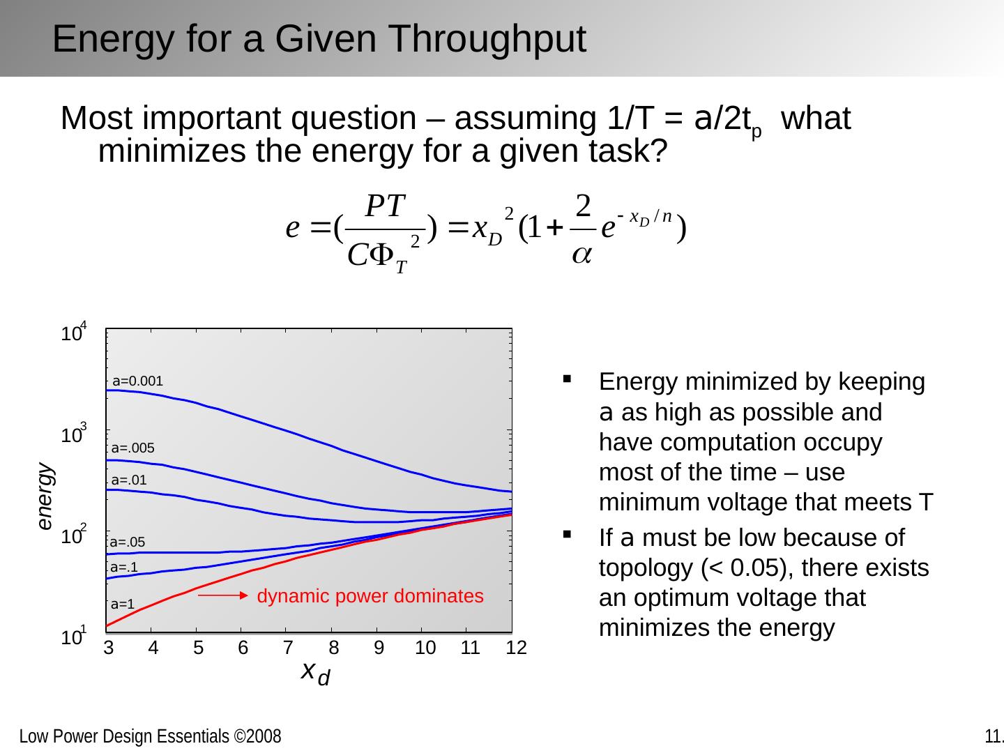
16 .Energy for a Given Throughput Most important question – assuming 1/T = a /2t p what minimizes the energy for a given task? 3 4 5 6 7 8 9 10 11 12 10 1 10 2 10 3 10 4 x d energy Energy minimized by keeping a as high as possible and have computation occupy most of the time – use minimum voltage that meets T If a must be low because of topology (< 0.05), there exists an optimum voltage that minimizes the energy a =1 a =.1 a =.05 a =.01 a =.005 a =0.001 dynamic power dominates
17 .Example: Energy-Aware FFT [Ref: A . Wang, ISSCC’04] Architecture scales gracefully from 128 to 1024 point lengths, and supports 8b and 16b precision. © IEEE 2004
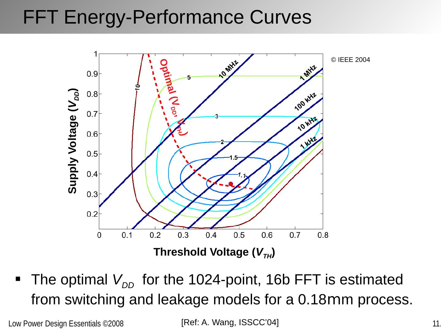
18 .FFT Energy-Performance Curves The optimal V DD for the 1024-point, 16b FFT is estimated from switching and leakage models for a 0.18 m m process. Optimal ( V DD , V TH ) Threshold Voltage ( V TH ) Supply Voltage ( V DD ) [Ref: A . Wang, ISSCC’04] © IEEE 2004
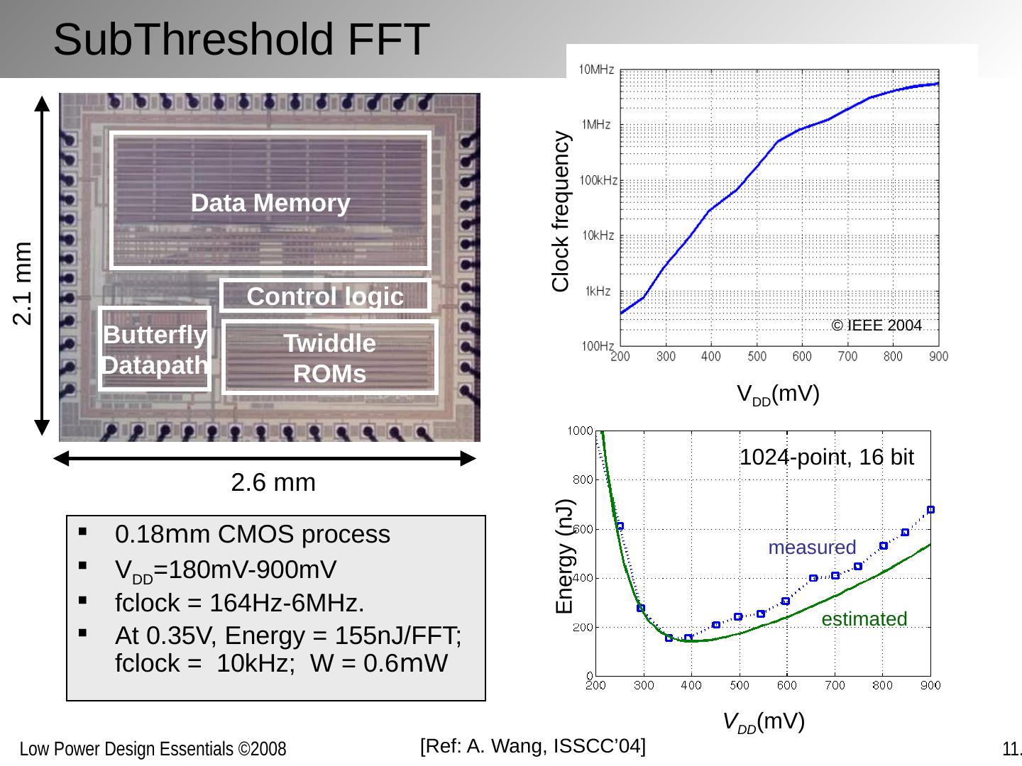
19 .SubThreshold FFT 0.18 m m CMOS process V DD =180mV-900mV fclock = 164Hz-6MHz. At 0.35V, Energy = 155nJ/FFT; fclock = 10kHz; W = 0.6 m W Data Memory Twiddle ROMs Butterfly Datapath Control logic 2.1 mm 2.6 mm V DD (mV) Clock frequency V DD (mV) 1024-point, 16 bit measured estimated Energy (nJ) [Ref: A . Wang, ISSCC’04] © IEEE 2004
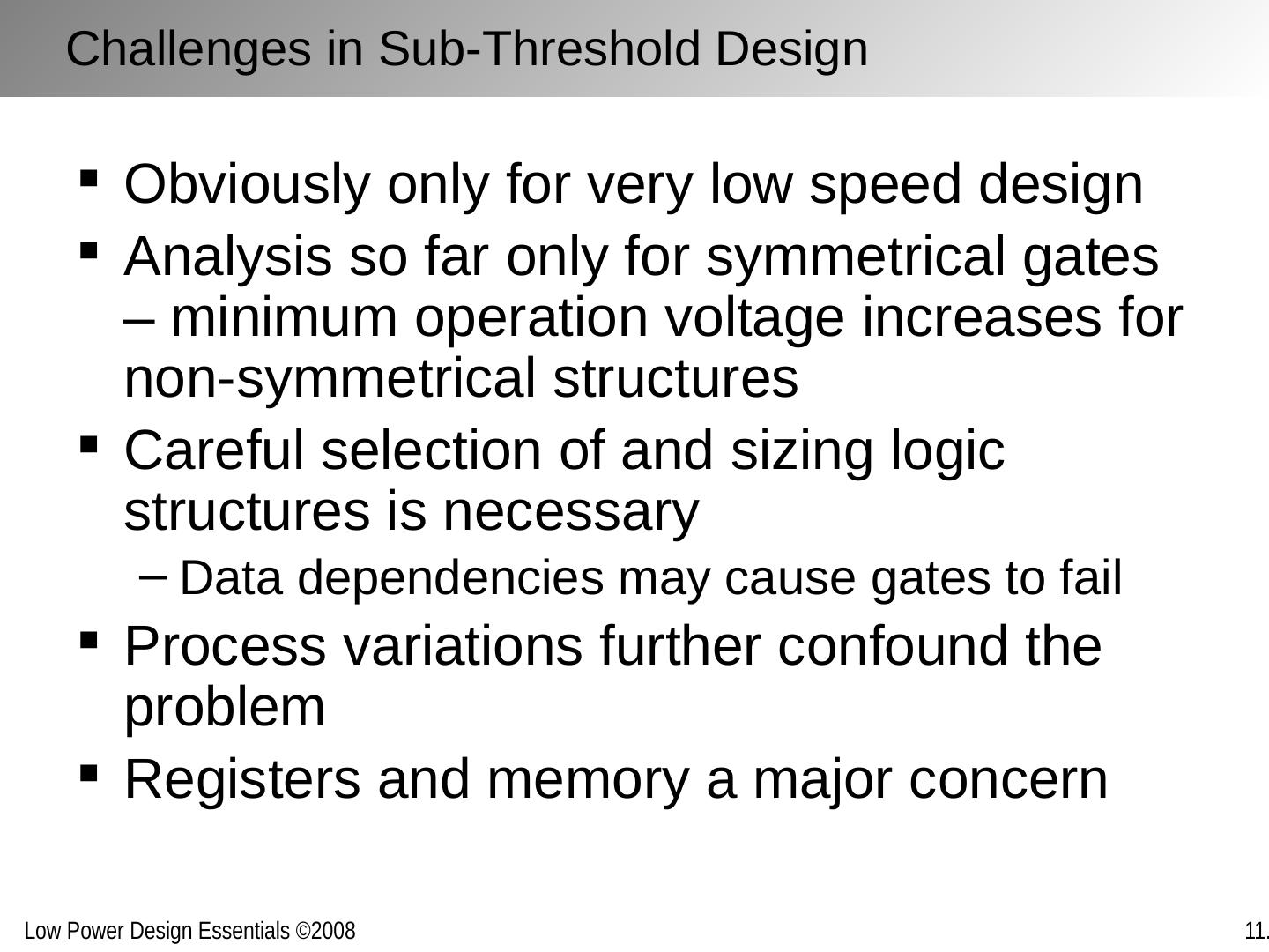
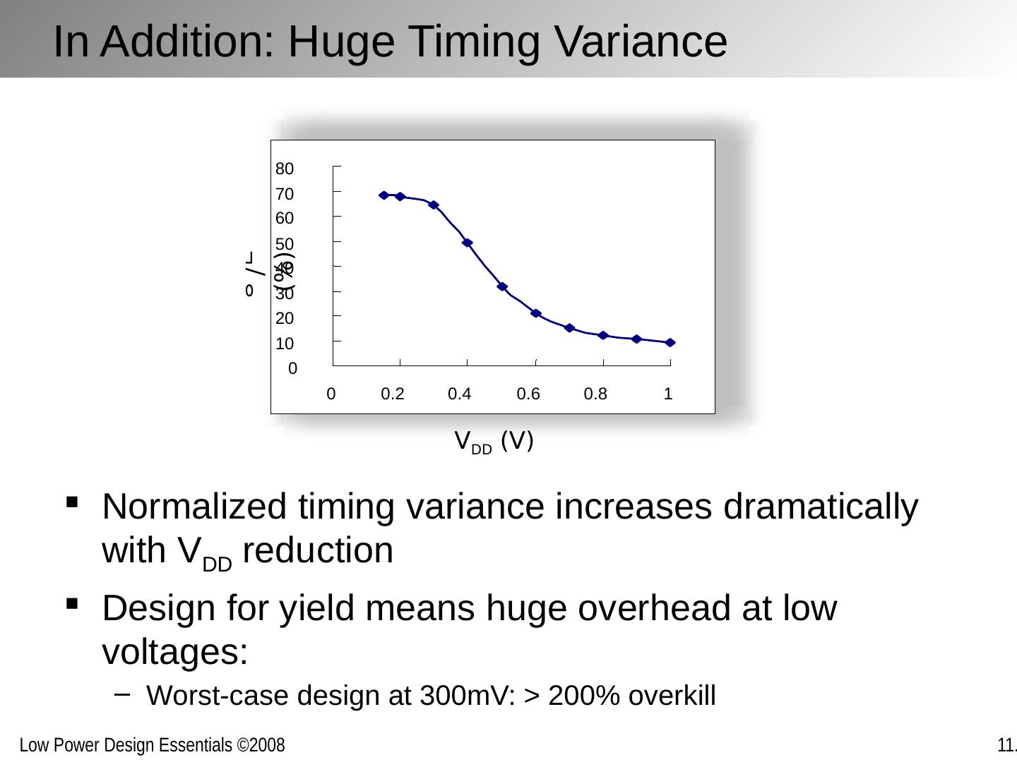
20 .Challenges in Sub-Threshold Design Obviously only for very low speed design Analysis so far only for symmetrical gates – minimum operation voltage increases for non-symmetrical structures Careful selection of and sizing logic structures is necessary Data dependencies may cause gates to fail Process variations further confound the problem Registers and memory a major concern
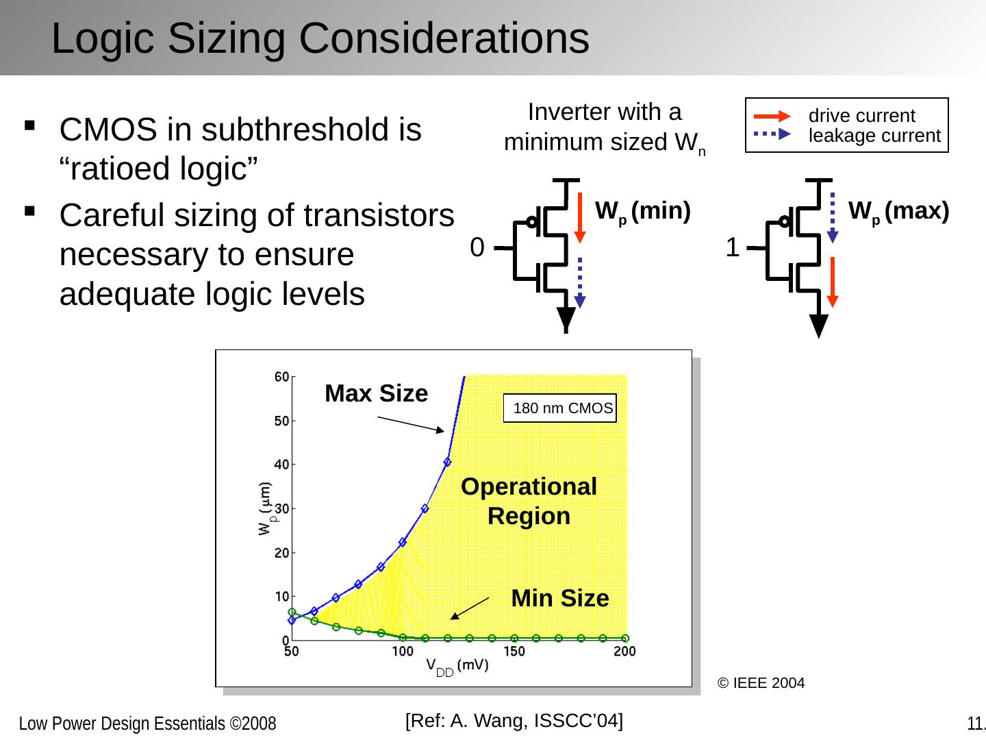
21 .Logic Sizing Considerations W p (max) Inverter with a minimum sized W n 0 1 W p (min) drive current leakage current CMOS in subthreshold is “ratioed logic” Careful sizing of transistors necessary to ensure adequate logic levels Max Size Min Size Operational Region [Ref: A . Wang, ISSCC’04] 180 nm CMOS © IEEE 2004
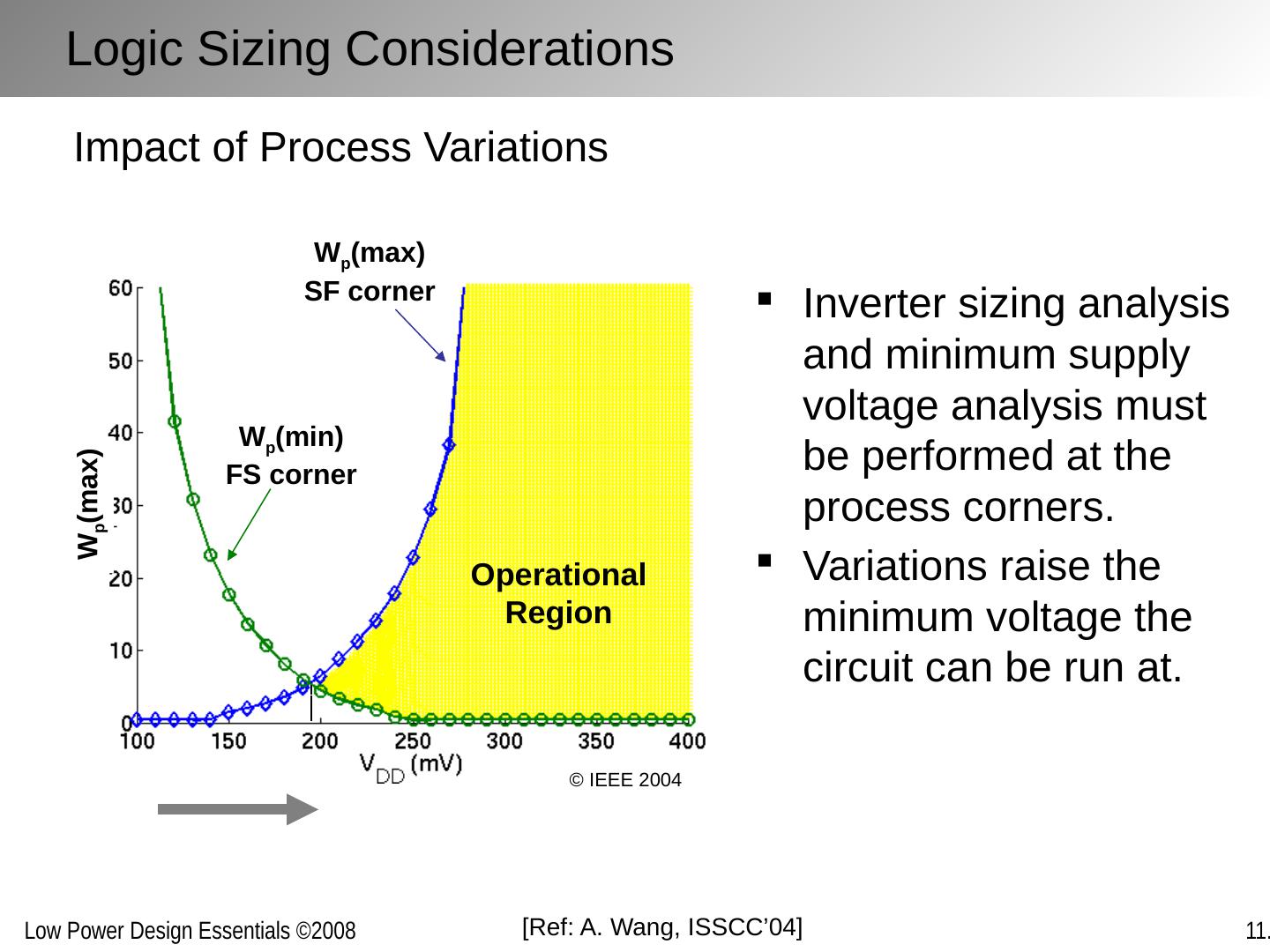
22 .Logic Sizing Considerations W p (max) SF corner W p (min) FS corner W p (max ) Inverter sizing analysis and minimum supply voltage analysis must be performed at the process corners. Variations raise the minimum voltage the circuit can be run at. Impact of Process Variations Operational Region [Ref: A . Wang, ISSCC’04] © IEEE 2004
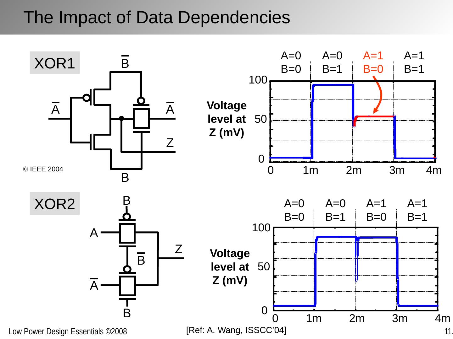
23 .The Impact of Data Dependencies B Z B A A XOR1 Z B B A B A XOR2 100 50 0 1m 2m 3m 4m 0 A=1 B=0 A=0 B=1 A=0 B=0 A=1 B=1 Voltage level at Z (mV) 50 0 Voltage level at Z (mV) 100 1m 2m 3m 4m 0 A=1 B=0 A=0 B=1 A=0 B=0 A=1 B=1 [Ref: A . Wang, ISSCC’04] © IEEE 2004
24 .The Impact of Data Dependencies idle current drive current A=1, B=0, Z=1 Z Leakage through the parallel devices causes XOR1 to fail at 100mV. XOR1 idle current drive current A=1, B=0, Z=1 weak drive current Z Balanced number of devices reduces the effects of leakage and process variations. XOR2 Solid sub-threshold design requires symmetry for all input vectors [Ref: A . Wang, ISSCC’04] © IEEE 2004
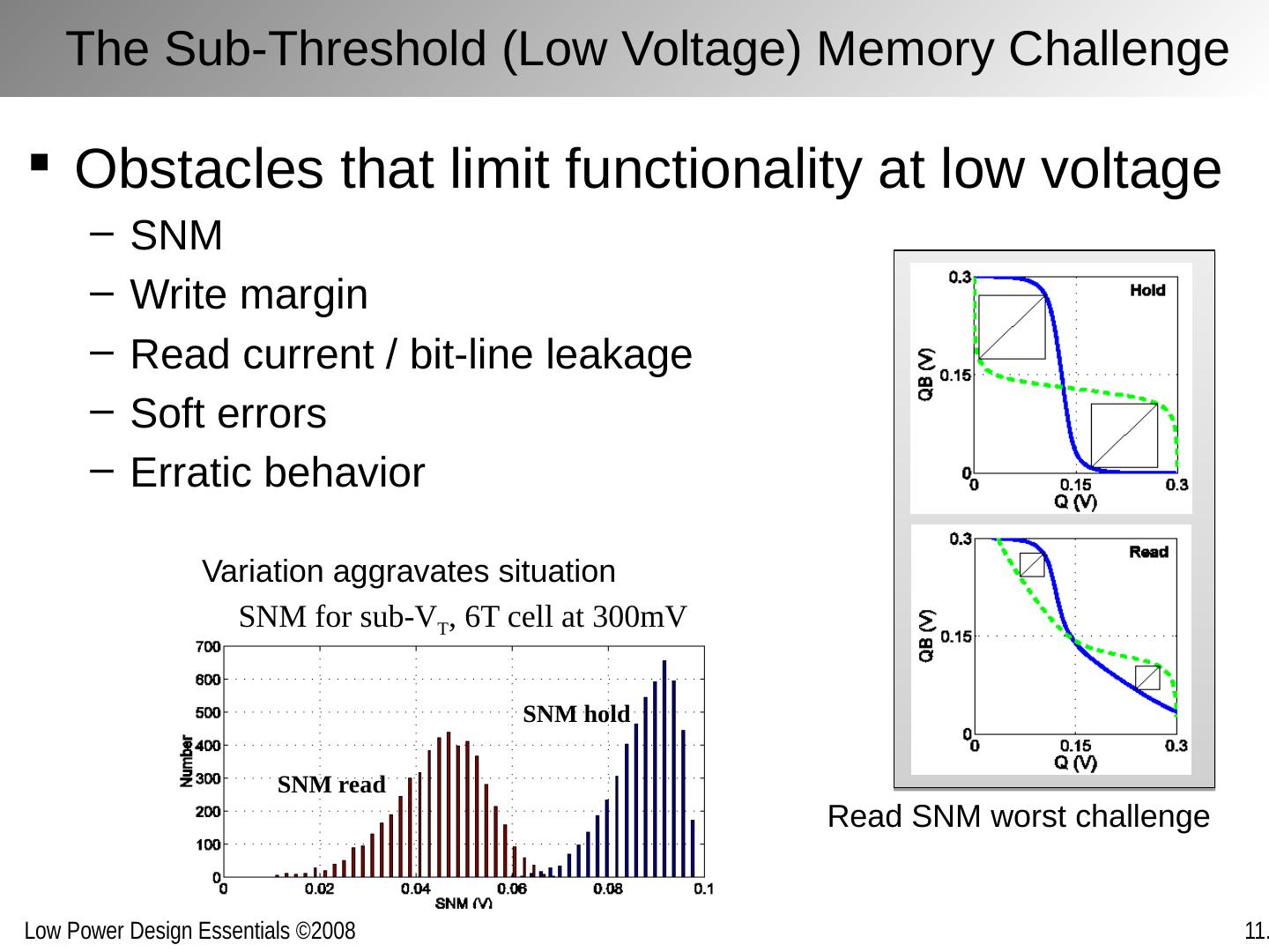
25 .The Sub-Threshold (Low Voltage) Memory Challenge Obstacles that limit functionality at low voltage SNM Write margin Read current / bit-line leakage Soft errors Erratic behavior Read SNM worst challenge SNM read SNM hold SNM for sub-V T , 6T cell at 300mV Variation aggravates situation
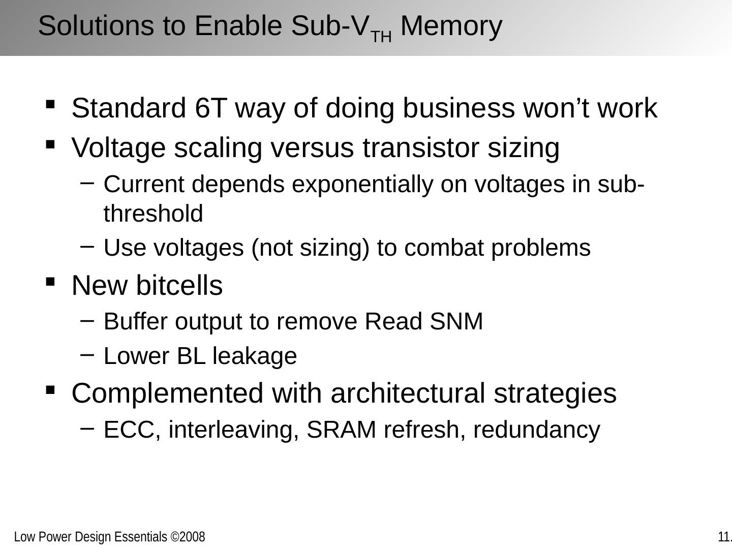
26 .Solutions to Enable Sub- V TH Memory Standard 6T way of doing business won’t work Voltage scaling versus transistor sizing Current depends exponentially on voltages in sub-threshold Use voltages (not sizing) to combat problems New bitcells Buffer output to remove Read SNM Lower BL leakage Complemented with architectural strategies ECC, interleaving, SRAM refresh, redundancy
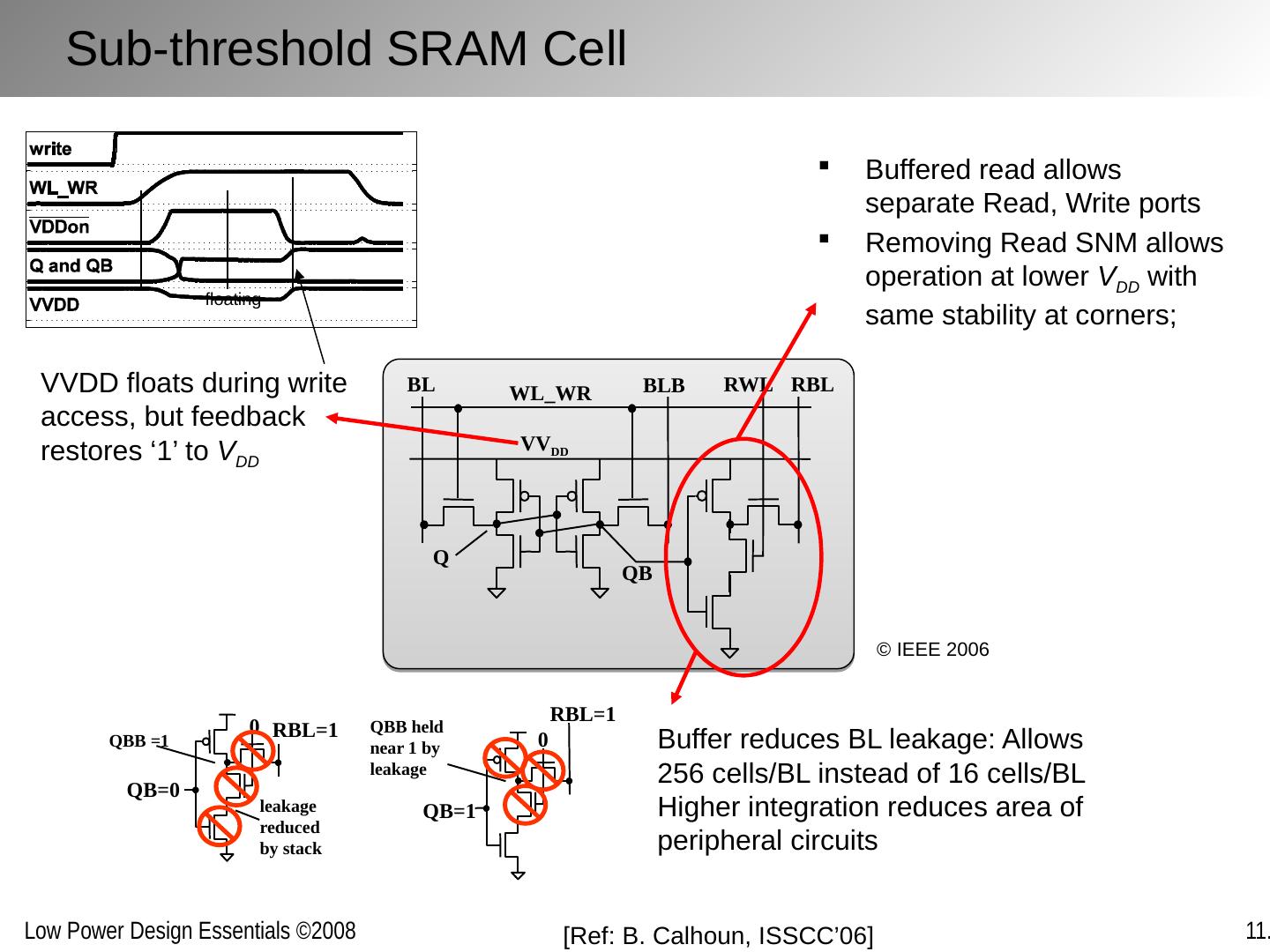
27 .Sub -threshold SRAM Cell [Ref: B. Calhoun, ISSCC’06 ] Buffered read allows separate Read, Write ports Removing Read SNM allows operation at lower V DD with same stability at corners; WL_WR BLB BL Q QB VV DD RBL RWL floating VVDD floats during write access, but feedback restores ‘1’ to V DD QB=1 RBL=1 0 QBB held near 1 by leakage QB=0 RBL=1 0 QBB =1 leakage reduced by stack Buffer reduces BL leakage: Allows 256 cells/BL instead of 16 cells/BL Higher integration reduces area of peripheral circuits © IEEE 2006
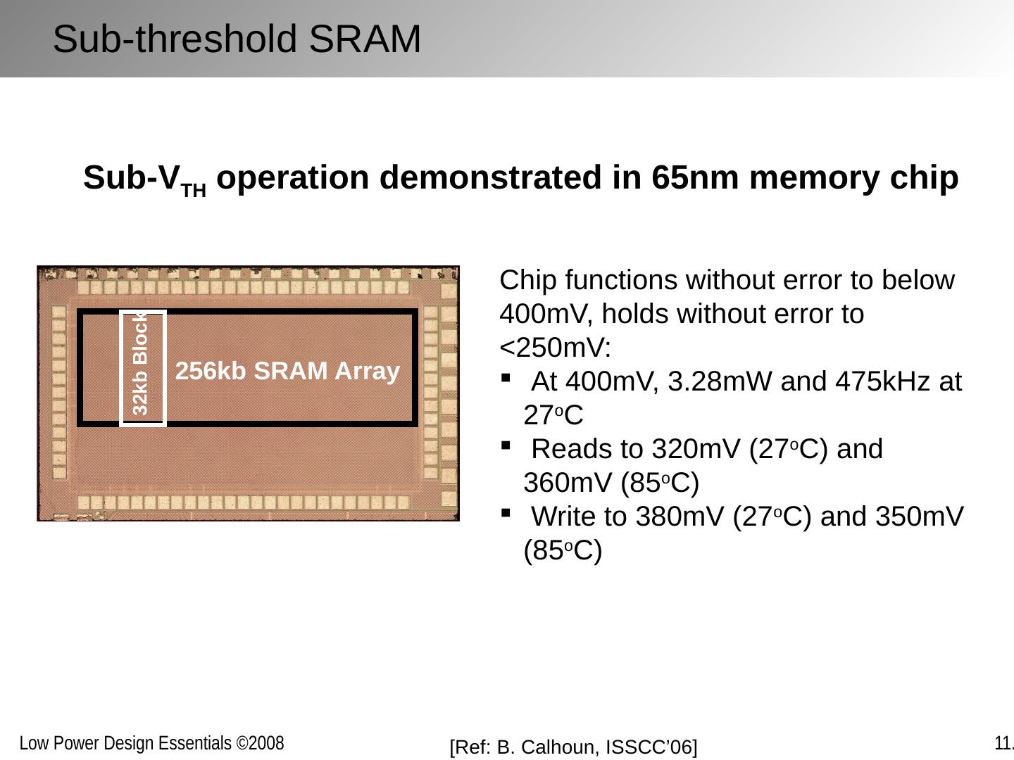
28 .Sub-threshold SRAM Chip functions without error to below 400mV, holds without error to <250mV: At 400mV, 3.28mW and 475kHz at 27 o C Reads to 320mV (27 o C) and 360mV (85 o C) Write to 380mV (27 o C) and 350mV (85 o C ) 256kb SRAM Array 32kb Block [Ref: B. Calhoun, ISSCC’06 ] Sub-V TH operation demonstrated in 65nm memory chip
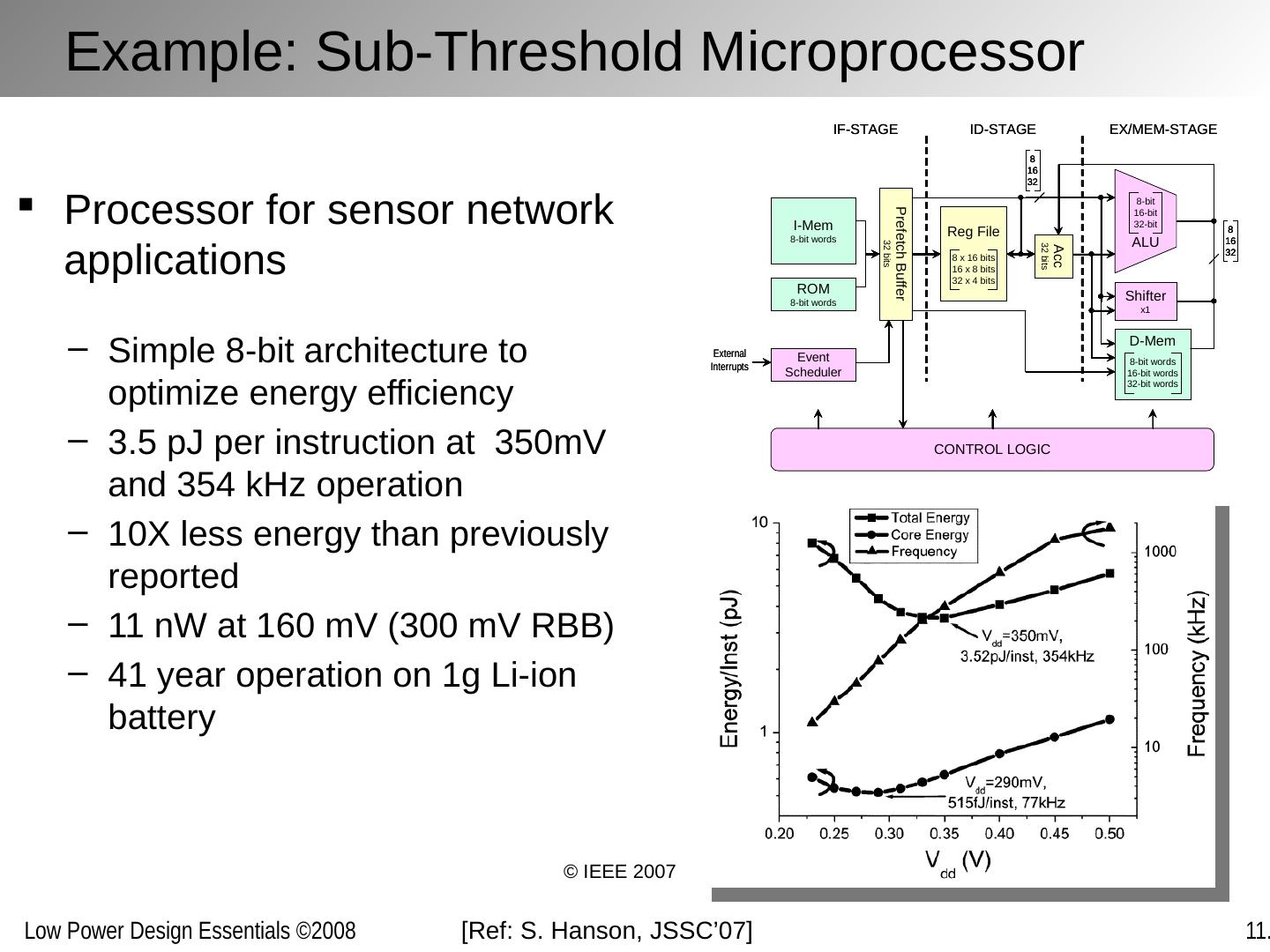
29 .Example: Sub-Threshold Microprocessor Processor for sensor network applications Simple 8-bit architecture to optimize energy efficiency 3.5 pJ per instruction at 350mV and 354 kHz operation 10X less energy than previously reported 11 nW at 160 mV (300 mV RBB) 41 year operation on 1g Li-ion battery [Ref: S. Hanson, JSSC’07] © IEEE 2007


