- 快召唤伙伴们来围观吧
- 微博 QQ QQ空间 贴吧
- 文档嵌入链接
- 复制
- 微信扫一扫分享
- 已成功复制到剪贴板
瞬态响应二极管的应用
展开查看详情
1 . Lecture #14 OUTLINE • pn Junctions: – transient response • turn-off • turn-on • pn diode applications Reading: Chapters 8 & 9 Spring 2003 EE130 Lecture 14, Slide 1 Transient Response of pn Diode • Suppose a pn-diode is forward biased, then suddenly turned off at time t = 0. Because of CD, the voltage across the pn junction depletion region cannot be changed instantaneously. (The delay in switching between the ON and OFF states is due to the time required to change the amount of excess minority carriers stored in the quasi-neutral regions.) Spring 2003 EE130 Lecture 14, Slide 2 1
2 . Turn-Off Transient • In order to turn the diode off, the excess minority carriers must be removed by net carrier flow out of the quasi-neutral regions and/or recombination – Carrier flow is limited by the switching circuitry Spring 2003 EE130 Lecture 14, Slide 3 Decay of Stored Charge Consider a p+n diode (Qp >> Qn): ∆pn(x) i(t) ts t vA(t) x xn dpn i For t > 0: =− >0 t dx x = xn qAD p ts Spring 2003 EE130 Lecture 14, Slide 4 2
3 . Examples (qualitative) Increase IF Increase IR Decrease τp i(t) i(t) i(t) ts ts ts t t t Spring 2003 EE130 Lecture 14, Slide 5 Storage Delay Time ts • ts is the primary “figure of merit” used to characterize the transient response of pn junction diodes dQ p Qp Qp =i− = − I R + 0+ ≤ t ≤ ts dt τp τ p • By separation of variables and integration from t = 0+ to t = ts, noting that I F = Q p (t = 0) / τ p and making the approximation Q p (t = t s ) = 0 IF We conclude that t s ≅ τ p ln1 + IR Spring 2003 EE130 Lecture 14, Slide 6 3
4 . Turn-On Transient Again, consider a p+n diode (Qp >> Qn): ∆pn(x) i(t) t vA(t) x xn dpn i For t > 0: =− <0 t dx x = xn qAD p Spring 2003 EE130 Lecture 14, Slide 7 dQ p Qp Qp =i− = IF − for t ≥ 0 + dt τp τp • By separation of variables and integration, we have ( Q p (t ) = I F τ p 1 − e −t / τ p ) • If we assume that the build-up of stored charge occurs quasi-statically so that ( Q p (t ) = I diffusion τ p = I 0 e qv A / kT − 1 τ p ) then v A (t ) = kT I F ln 1 + q I0 1− e p ( −t / τ ) Spring 2003 EE130 Lecture 14, Slide 8 4
5 . • If τp is large, then the time required to turn on the diode is approximately ∆Q/IF where ∆Q = ∆Q p + ∆Q j Spring 2003 EE130 Lecture 14, Slide 9 Summary of Important Concepts • Under forward bias, minority carriers are injected into the quasi-neutral regions of the diode • Current flowing across junction is comprised of hole and electron components • In order for one of these components to be dominant, the junction must be asymmetrically doped Spring 2003 EE130 Lecture 14, Slide 10 5
6 . Summary of Important Concepts (cont.) • The ideal diode equation stipulates the relationship between JN(-xp) and JP(xn) ¾ If holes are forced to flow across a forward-biased junction, then electrons must also be injected across the junction Spring 2003 EE130 Lecture 14, Slide 11 Summary of Important Concepts (cont.) • Under reverse bias, minority carriers are collected into the quasi-neutral regions of the diode • Minority carriers within a diffusion length of the depletion region will diffuse into the depletion region and then be swept across the junction by the electric field. → Current flowing in a reverse-biased diode depends on the rate at which minority carriers are supplied in the quasi-neutral regions Spring 2003 EE130 Lecture 14, Slide 12 6
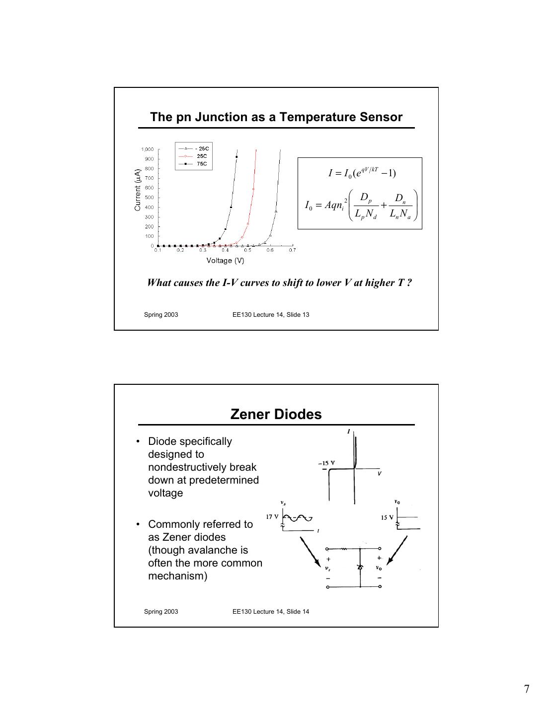
7 . The pn Junction as a Temperature Sensor I = I 0 (e qV kT − 1) Dp D I 0 = Aqni + n 2 L N p d Ln N a What causes the I-V curves to shift to lower V at higher T ? Spring 2003 EE130 Lecture 14, Slide 13 Zener Diodes • Diode specifically designed to nondestructively break down at predetermined voltage • Commonly referred to as Zener diodes (though avalanche is often the more common mechanism) Spring 2003 EE130 Lecture 14, Slide 14 7
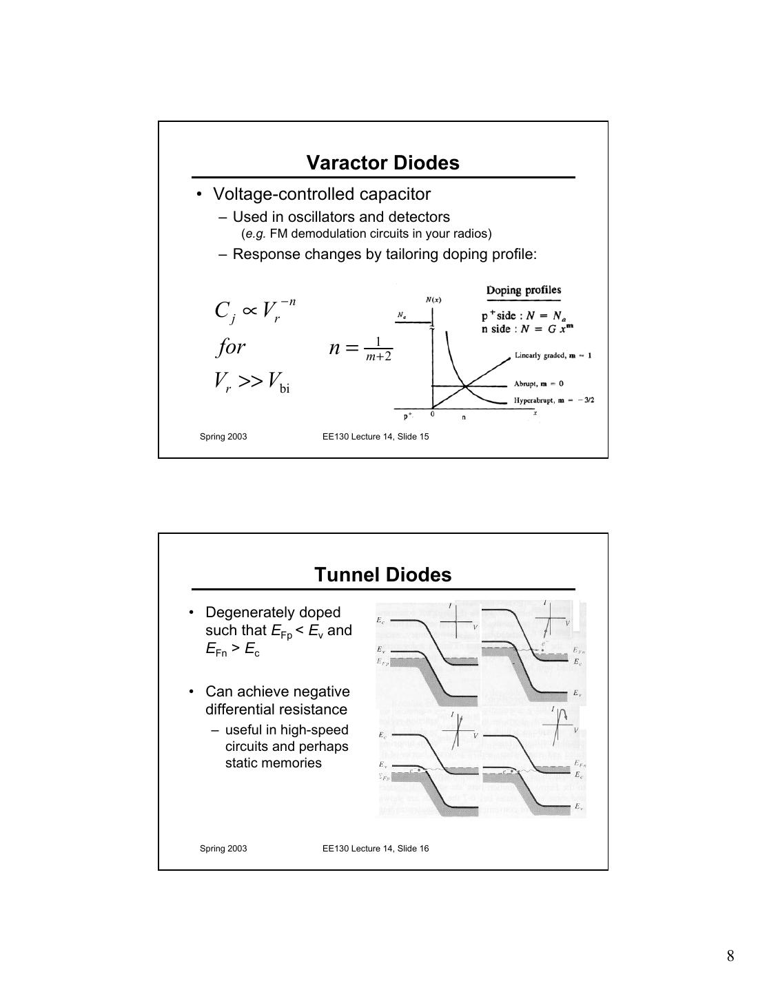
8 . Varactor Diodes • Voltage-controlled capacitor – Used in oscillators and detectors (e.g. FM demodulation circuits in your radios) – Response changes by tailoring doping profile: −n C j ∝ Vr for n= 1 m+2 Vr >> Vbi Spring 2003 EE130 Lecture 14, Slide 15 Tunnel Diodes • Degenerately doped such that EFp < Ev and EFn > Ec • Can achieve negative differential resistance – useful in high-speed circuits and perhaps static memories Spring 2003 EE130 Lecture 14, Slide 16 8
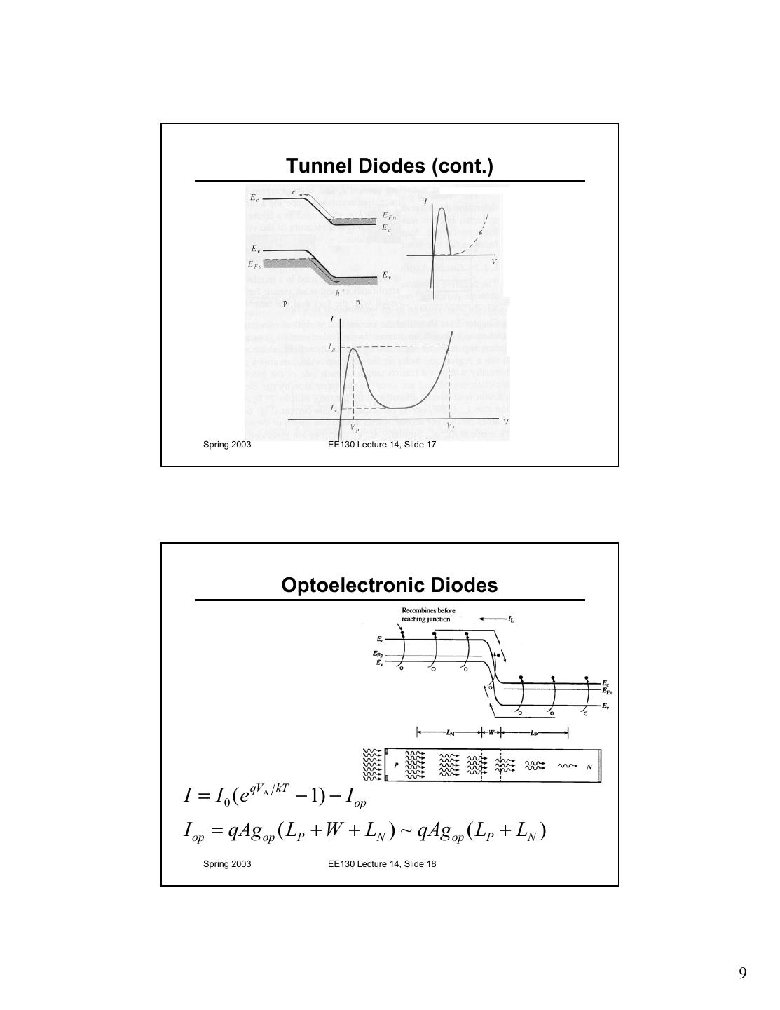
9 . Tunnel Diodes (cont.) Spring 2003 EE130 Lecture 14, Slide 17 Optoelectronic Diodes I = I 0 ( e qVA kT − 1) − I op I op = qAg op ( LP + W + LN ) ~ qAg op ( LP + LN ) Spring 2003 EE130 Lecture 14, Slide 18 9
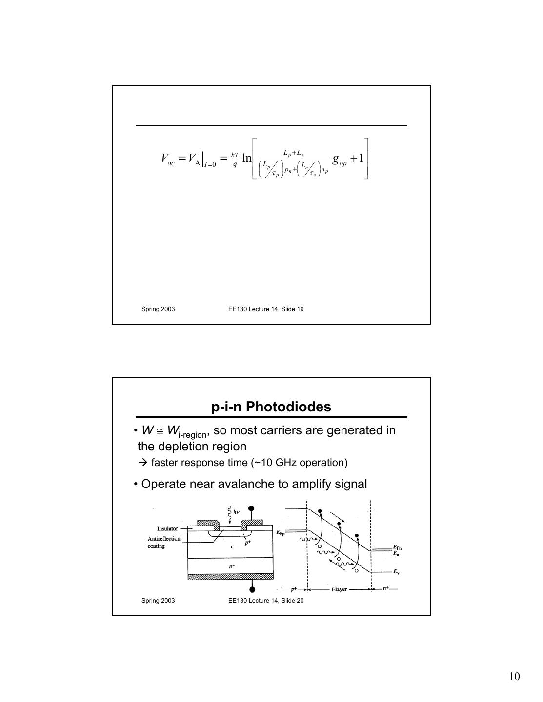
10 . L +L Voc = VA I =0 = kT q ln L p p nL g op + 1 τ p pn + n τ n n p Spring 2003 EE130 Lecture 14, Slide 19 p-i-n Photodiodes • W ≅ Wi-region, so most carriers are generated in the depletion region Æ faster response time (~10 GHz operation) • Operate near avalanche to amplify signal Spring 2003 EE130 Lecture 14, Slide 20 10
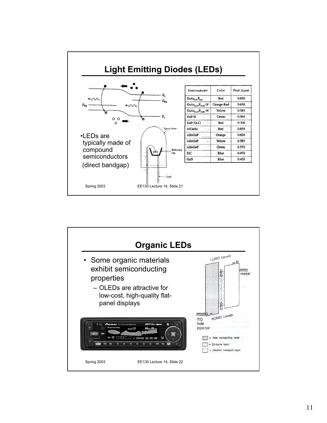
11 . Light Emitting Diodes (LEDs) •LEDs are typically made of compound semiconductors (direct bandgap) Spring 2003 EE130 Lecture 14, Slide 21 Organic LEDs • Some organic materials exhibit semiconducting properties – OLEDs are attractive for low-cost, high-quality flat- panel displays Spring 2003 EE130 Lecture 14, Slide 22 11


