- 快召唤伙伴们来围观吧
- 微博 QQ QQ空间 贴吧
- 文档嵌入链接
- 复制
- 微信扫一扫分享
- 已成功复制到剪贴板
电路及能源基础
展开查看详情
1 .Power and Energy Basics
2 .Chapter Outline Metrics Dynamic power Static power Energy-delay trade-off’s
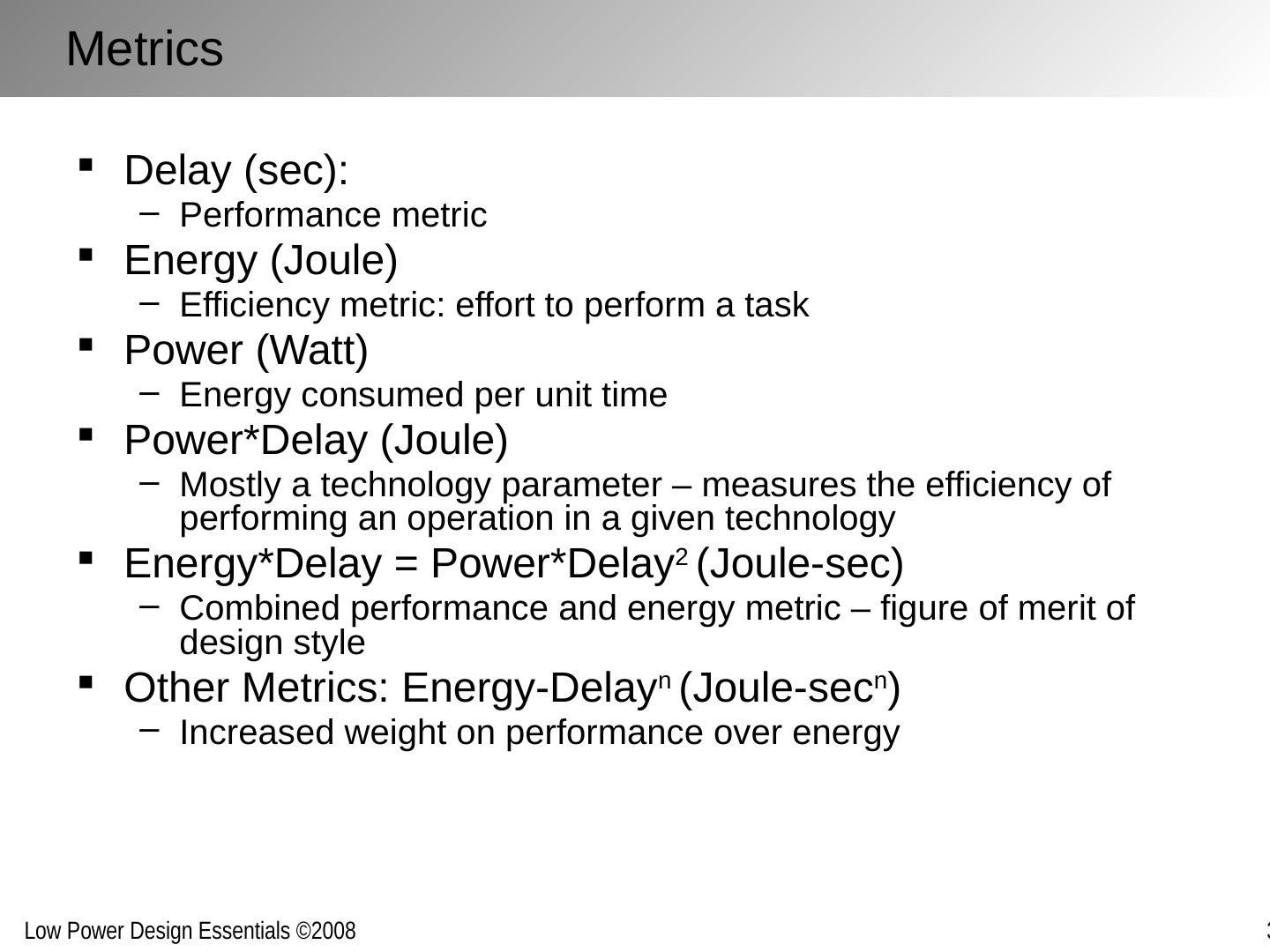
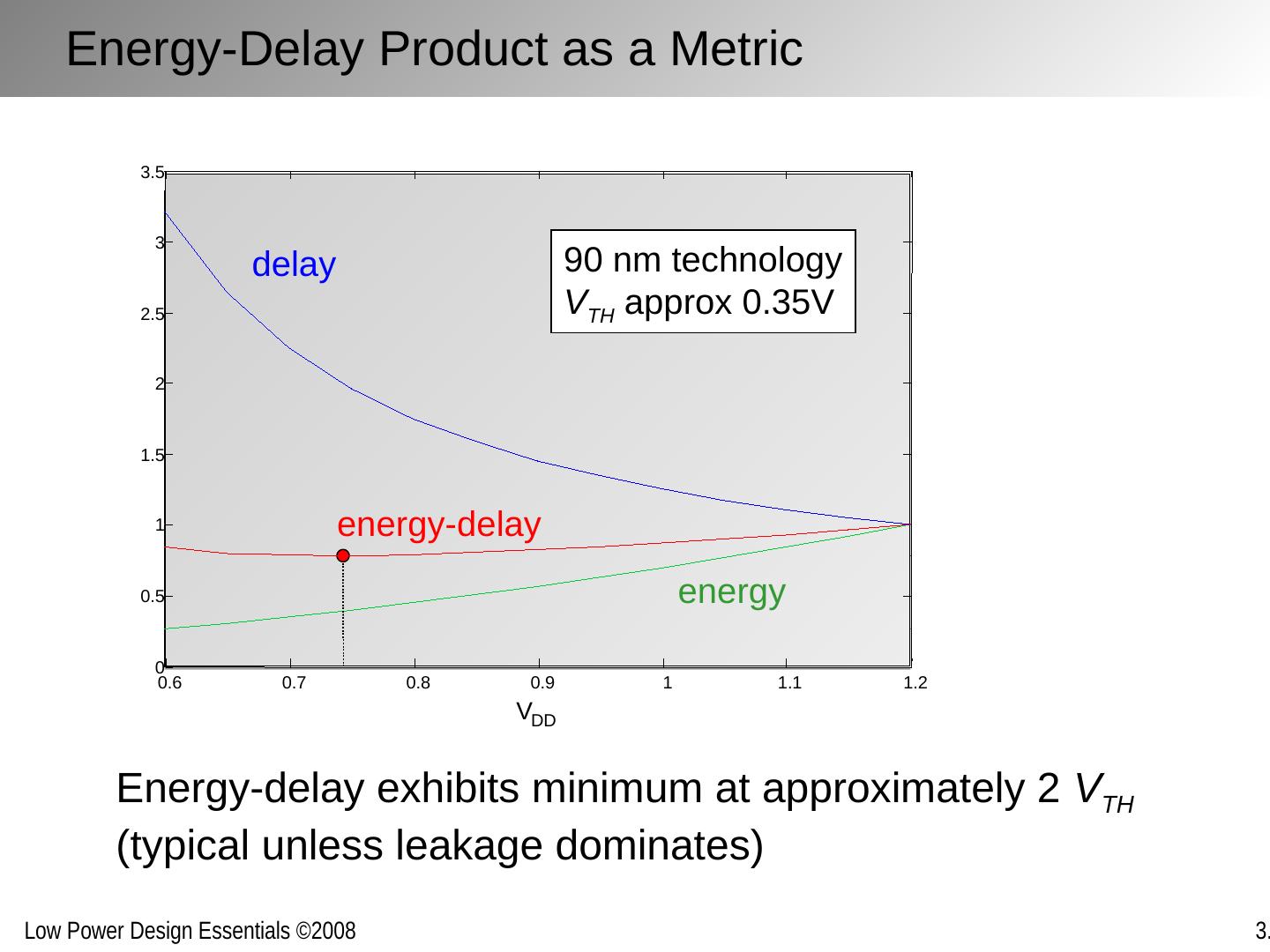
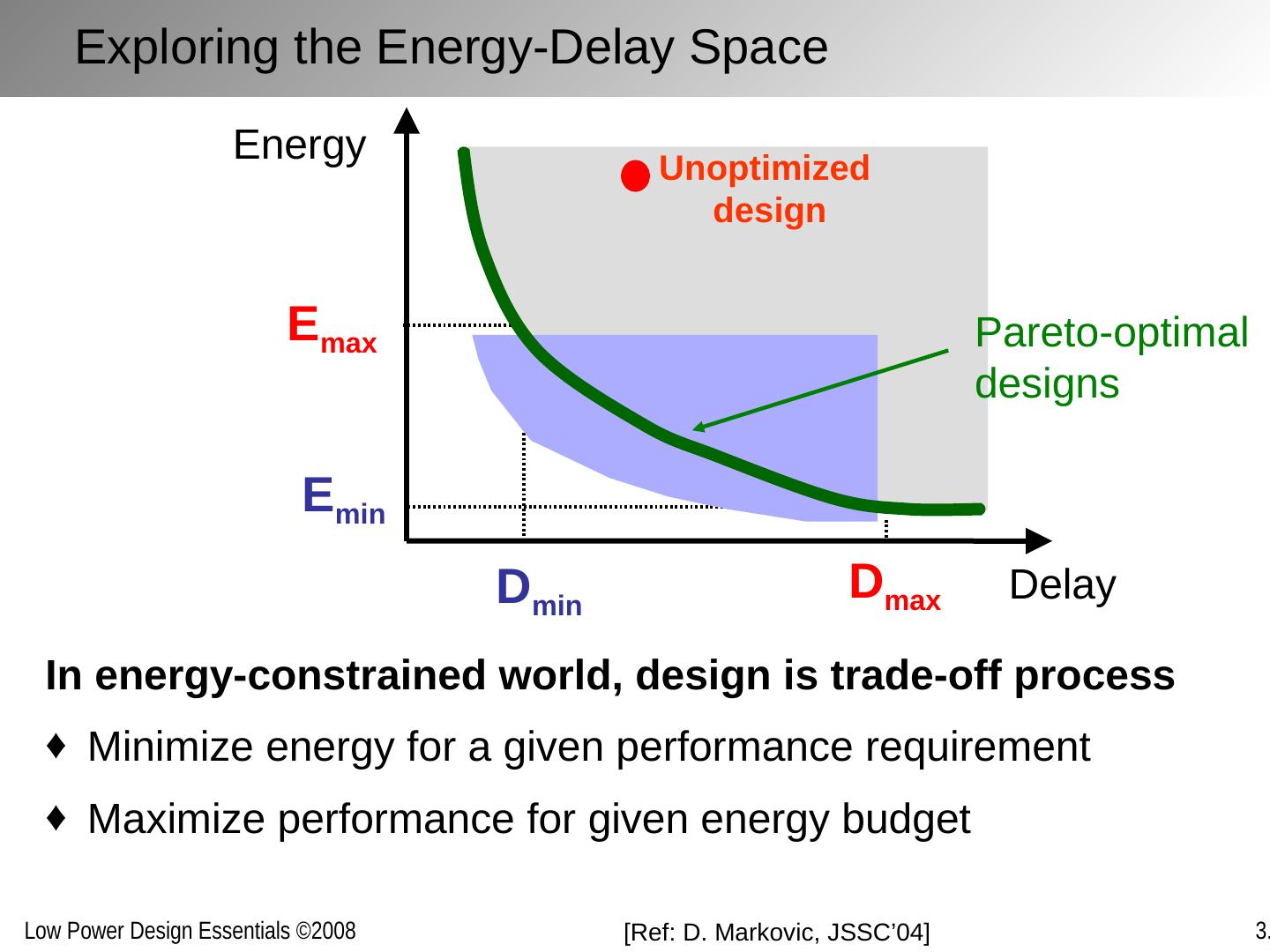
3 .Metrics Delay (sec): Performance metric Energy (Joule) Efficiency metric: effort to perform a task Power (Watt) Energy consumed per unit time Power * Delay (Joule) Mostly a technology parameter – measures the efficiency of performing an operation in a given technology Energy*Delay = Power*Delay 2 (Joule-sec) Combined performance and energy metric – figure of merit of design style Other Metrics: Energy- Delay n (Joule- sec n ) Increased weight on performance over energy
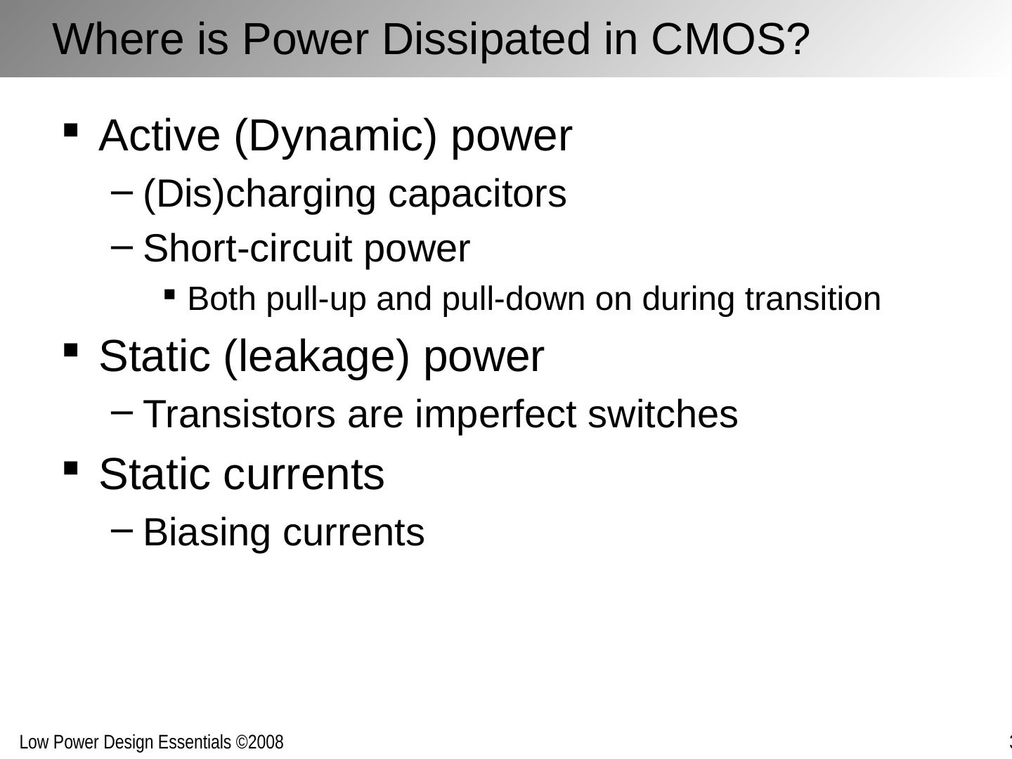
4 .Where is Power Dissipated in CMOS? Active (Dynamic) power ( Dis)charging capacitors Short-circuit power Both pull-up and pull-down on during transition Static (leakage) power Transistors are imperfect switches Static currents Biasing currents
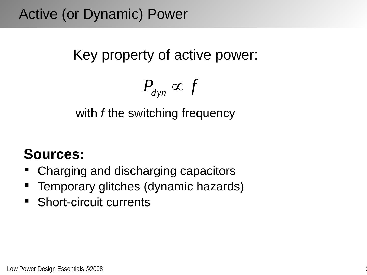
5 .Active (or Dynamic) Power Sources: Charging and discharging capacitors Temporary glitches (dynamic hazards) Short-circuit currents Key property of active power: with f the switching frequency
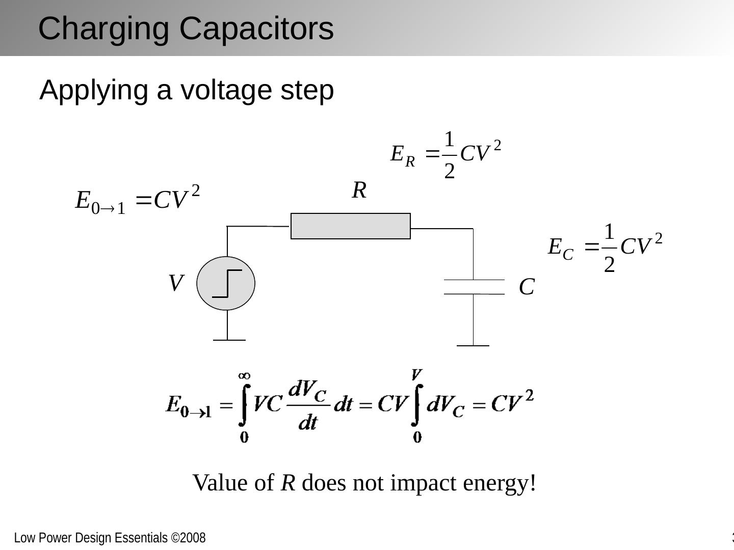
6 .Charging Capacitors R C V Applying a voltage step Value of R does not impact energy!
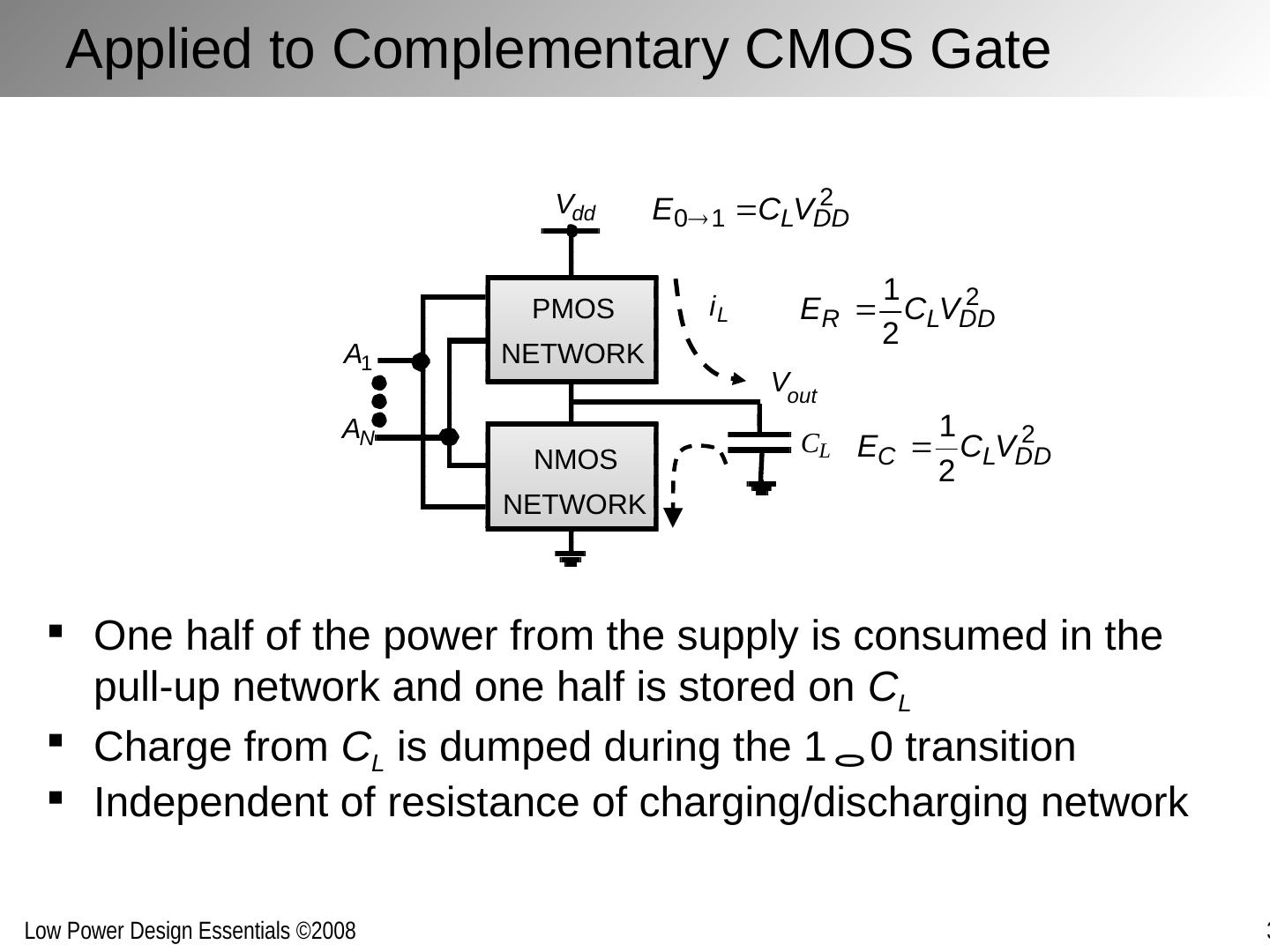
7 .Applied to Complementary CMOS Gate One half of the power from the supply is consumed in the pull-up network and one half is stored on C L Charge from C L is dumped during the 1 0 transition Independent of resistance of charging/discharging network V dd V out i L C L PMOS NETWORK NMOS A 1 A N NETWORK
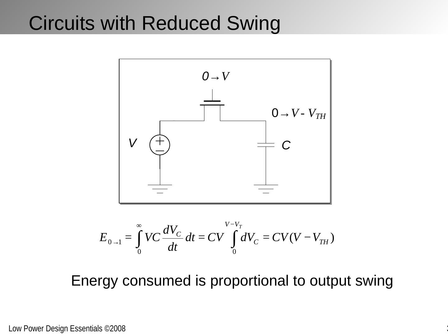
8 .Circuits with Reduced Swing Energy consumed is proportional to output swing
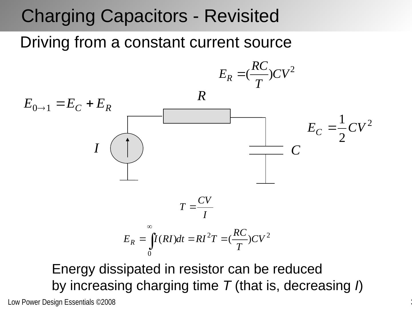
9 .Charging Capacitors - Revisited R C I Driving from a constant current source Energy dissipated in resistor can be reduced by increasing charging time T (that is, decreasing I )
10 .Charging Capacitors Using constant voltage or current driver? Energy dissipated using constant current charging can be made arbitrarily small at the expense of delay: Adiabatic charging E constant_current < E constant_voltage if T > 2 RC Note: t p (RC) = 0.69 RC t 0 →90% (RC) = 2.3 RC
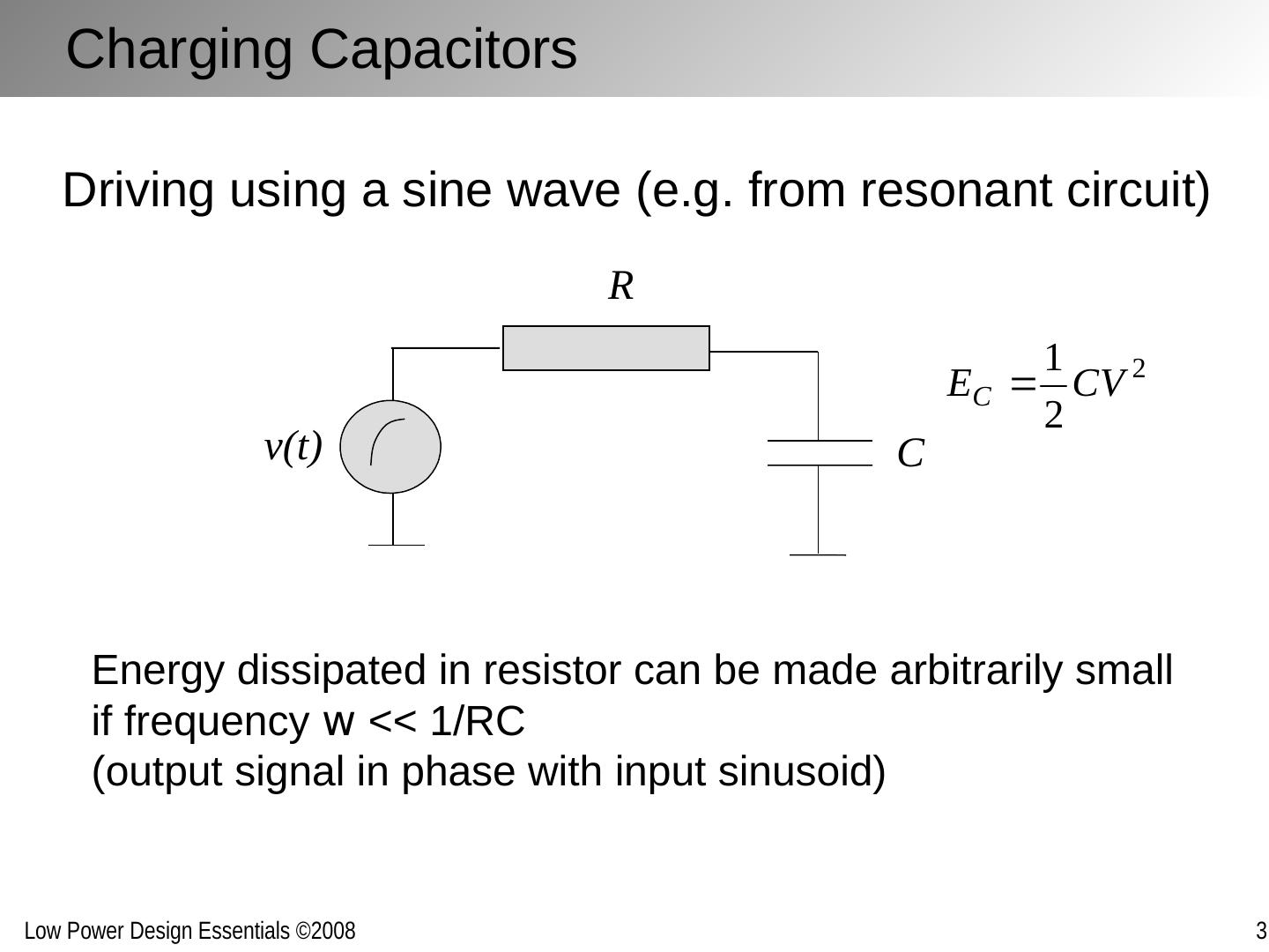
11 .Charging Capacitors Driving using a sine wave (e.g. from resonant circuit) Energy dissipated in resistor can be made arbitrarily small if frequency w << 1/RC (output signal in phase with input sinusoid) R C v(t)
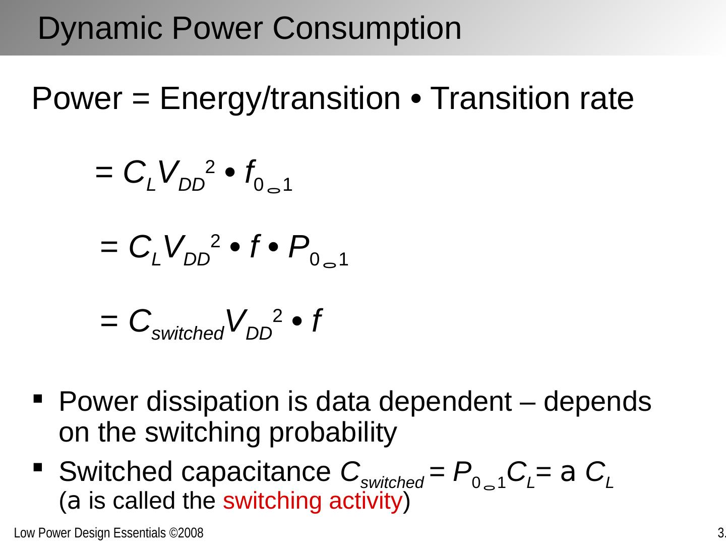
12 .Dynamic Power Consumption Power = Energy/transition • Transition rate = C L V DD 2 • f 0 1 = C L V DD 2 • f • P 0 1 = C switched V DD 2 • f Power dissipation is data dependent – depends on the switching probability Switched capacitance C switched = P 0 1 C L = a C L ( a is called the switching activity )
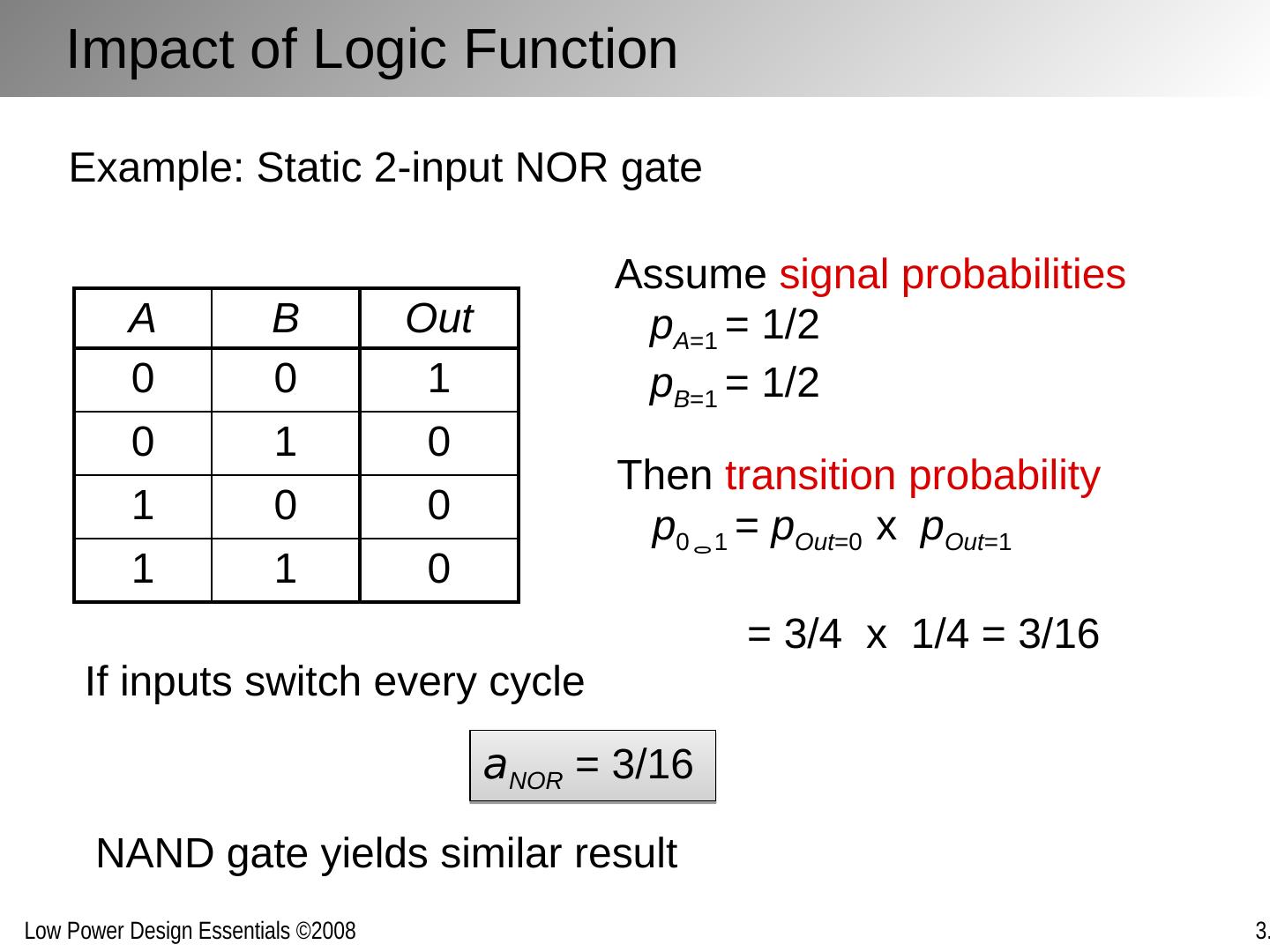
13 .Impact of Logic Function A B Out 0 0 1 0 1 0 1 0 0 1 1 0 Example: Static 2-input NOR gate Assume signal probabilities p A =1 = 1/2 p B =1 = 1/2 Then transition probability p 01 = p Out =0 x p Out =1 = 3/4 x 1/4 = 3/16 a NOR = 3/16 If inputs switch every cycle NAND gate yields similar result
14 .Impact of Logic Function A B Out 0 0 0 0 1 1 1 0 1 1 1 0 Example: Static 2-input XOR Gate Assume signal probabilities p A =1 = 1/2 p B =1 = 1/2 Then transition probability p 01 = p Out =0 x p Out =1 = 1/2 x 1/2 = 1/4 P 01 = 1/4 If inputs switch in every cycle
15 .Transition Probabilities for Basic Gates p 01 AND (1 - p A p B ) p A p B OR (1 - p A )(1 - p B )(1 - (1 - p A )(1 - p B )) XOR (1 - ( p A + p B – 2 p A p B ))( p A + p B – 2 p A p B ) Activity for static CMOS gates a = p 0 p 1 As a function of the input probabilities
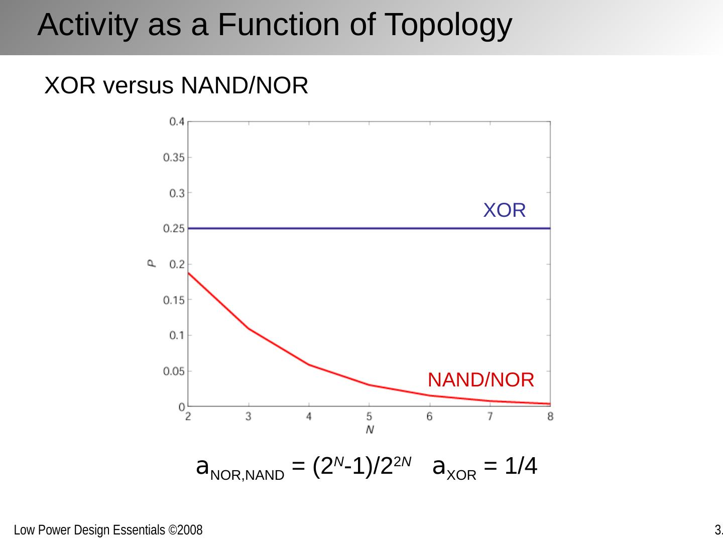
16 .Activity as a Function of Topology a NOR,NAND = (2 N -1)/2 2 N a XOR = 1/4 XOR versus NAND/NOR XOR NAND/NOR
17 .How about Dynamic Logic? Energy dissipated when effective output is zero! or P 0 →1 = P 0 V DD Eval Precharge Always larger than P 0 P 1 ! Activity in dynamic circuits hence always higher than static. But … capacitance most often smaller. E.g. P 0 → 1 (NAND) = 1/2 N ; P 0 → 1 (NOR) = (2 N -1)/2 N
18 .Differential Logic? V DD Out Out Gate Static: Activity is doubled Dynamic: Transition probability is 1! Hence: power always increases.
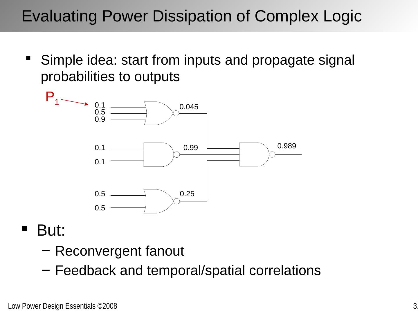
19 .Evaluating Power Dissipation of Complex Logic Simple idea: start from inputs and propagate signal probabilities to outputs But: Reconvergent fanout Feedback and temporal/spatial correlations P 1
20 .Reconvergent Fanout (Spatial Correlation) P Z = 1- P A . P ( X | A ) = 1 Becomes complex and intractable real fast Inputs to gate can be interdependent (correlated) no reconvergence P Z = 1-(1-P A )P B reconvergent P Z = 1-(1-P A )P A ? NO! P Z = 1 reconvergence Must use conditional probabilities P Z : probability that Z=1 probability that X=1 given that A=1
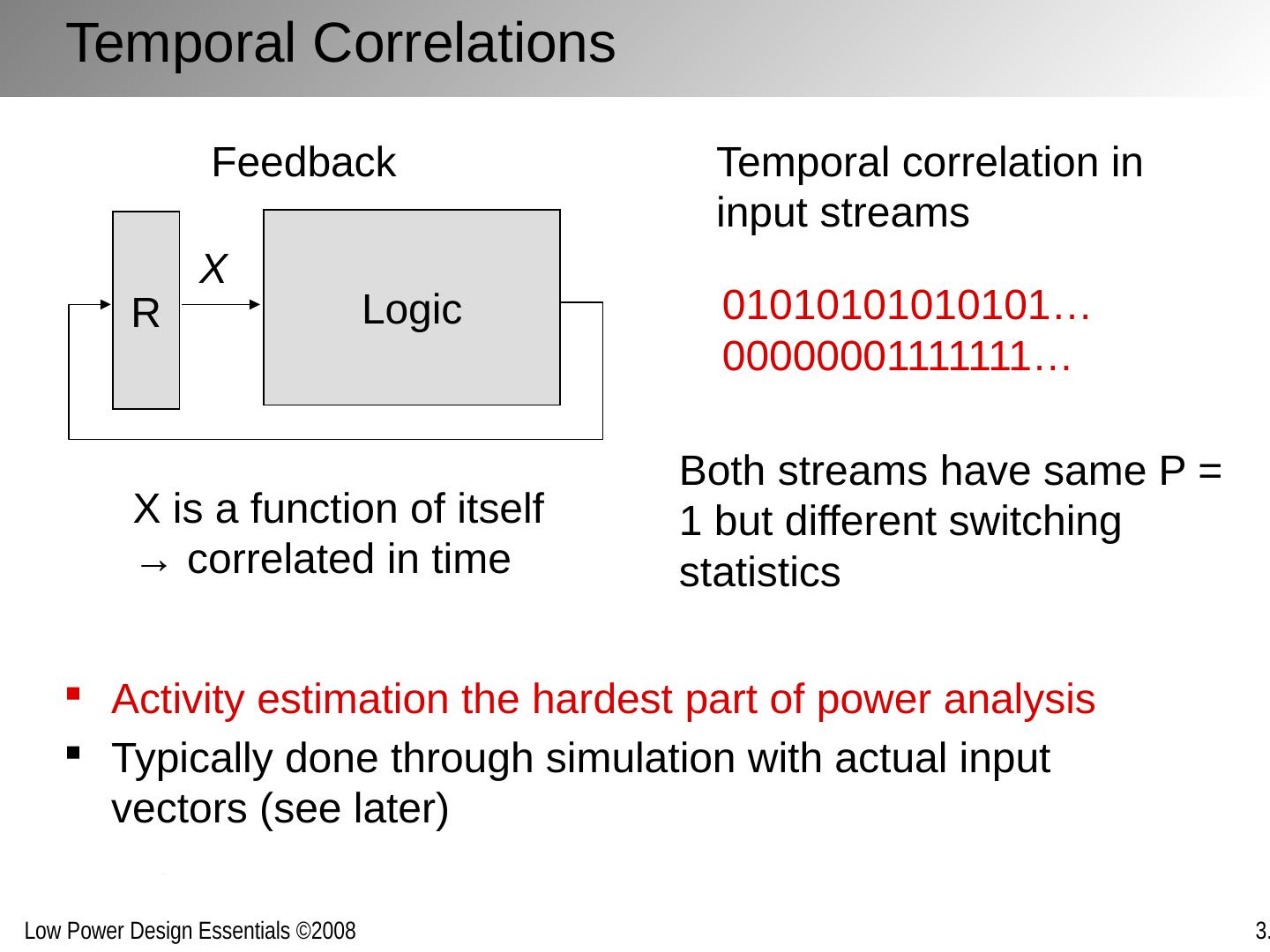
21 .Temporal Correlations Activity estimation the hardest part of power analysis Typically done through simulation with actual input vectors (see later) R Logic X Feedback X is a function of itself → correlated in time Temporal correlation in input streams 01010101010101… 00000001111111… Both streams have same P = 1 but different switching statistics
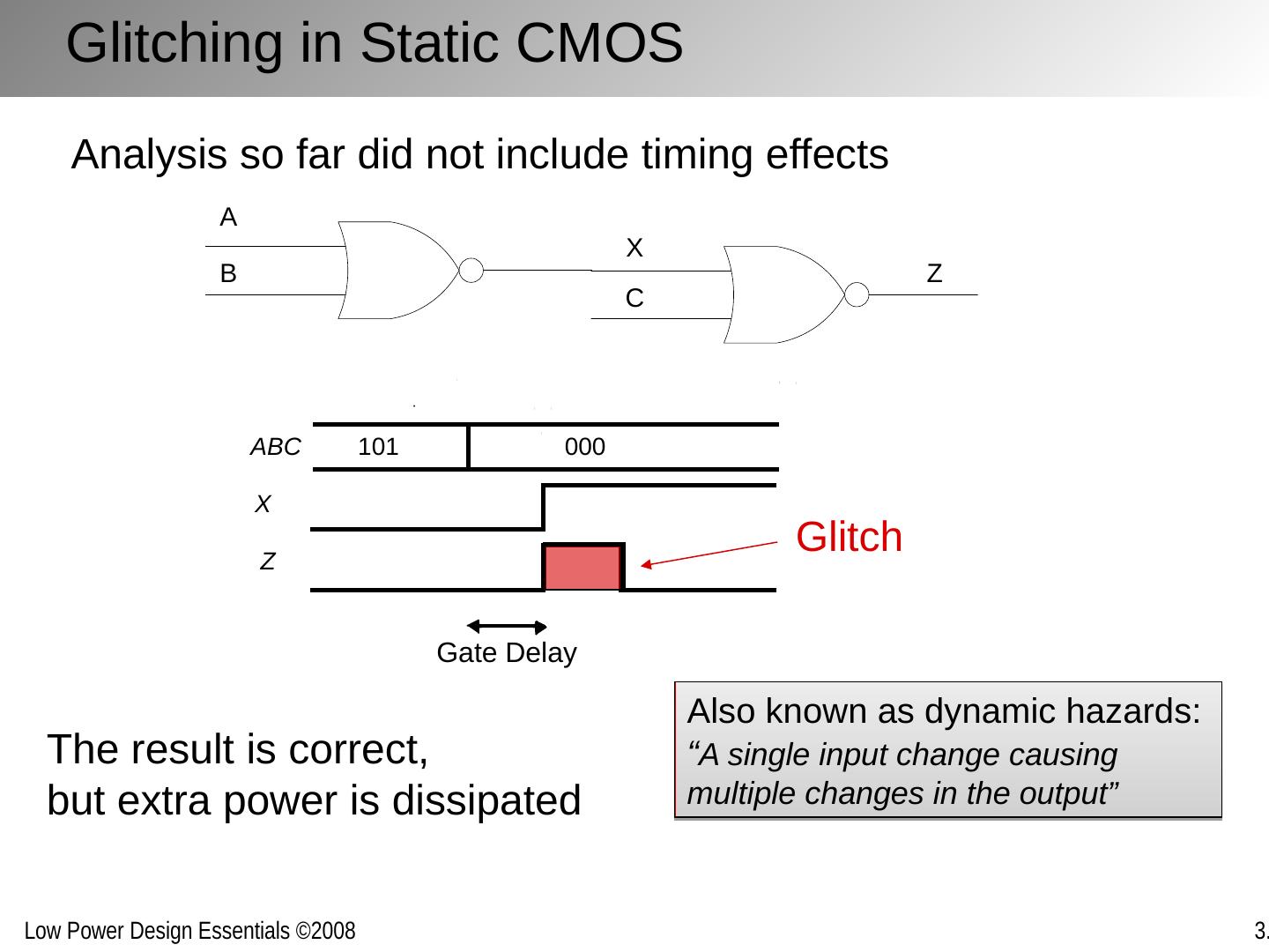
22 .Glitching in Static CMOS ABC 101 000 X Z Gate Delay The result is correct, but extra power is dissipated Glitch Analysis so far did not include timing effects Also known as dynamic hazards: “ A single input change causing multiple changes in the output”
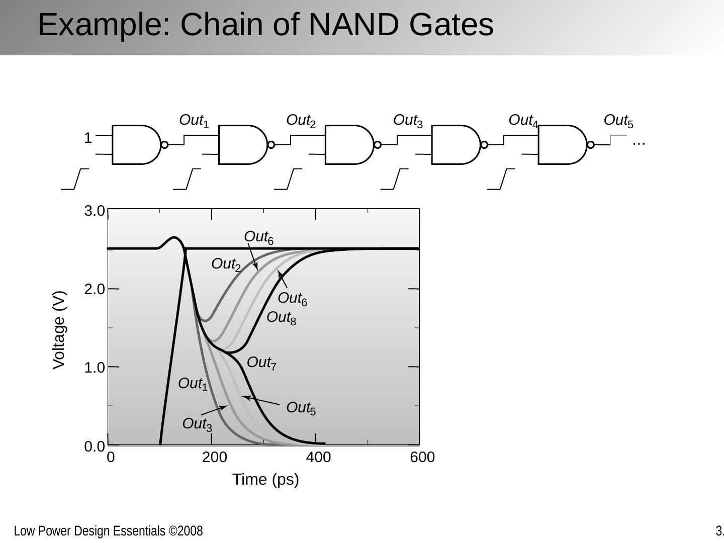
23 .Example: Chain of NAND Gates 1 Out 1 Out 2 Out 3 Out 4 Out 5 0 200 400 600 0.0 1.0 2.0 3.0 Time ( ps ) Out 8 Out 6 Out 2 Out 6 Out 1 Out 3 Out 7 Out 5 Voltage (V)
24 .What Causes Glitches? A,B C,D X Y Z A,B C,D X Y Z Uneven arrival times of input signals of gate due to unbalanced delay paths Solution: balancing delay paths!
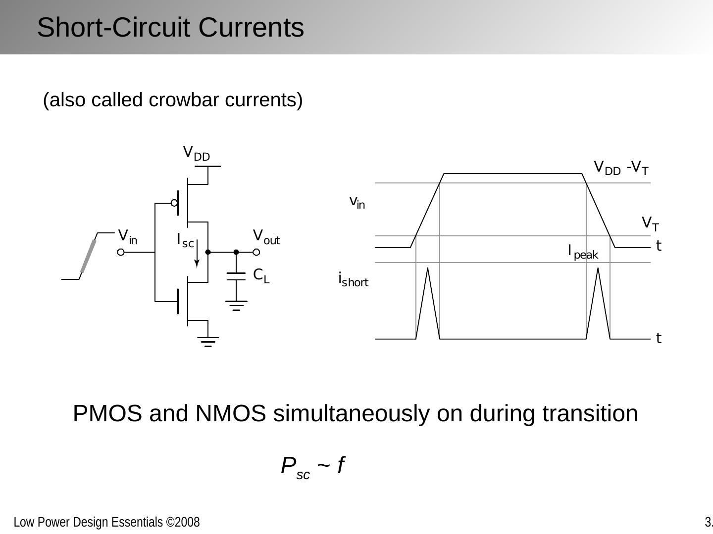
25 .Short-Circuit Currents (also called crowbar currents) PMOS and NMOS simultaneously on during transition P sc ~ f
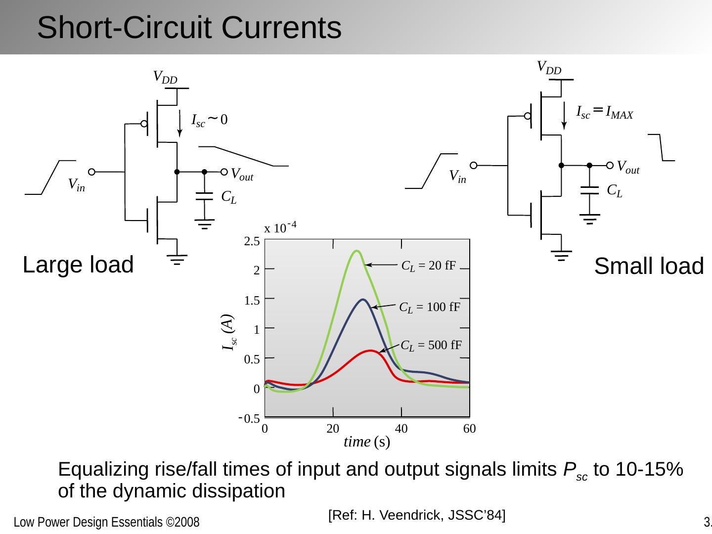
26 .Short-Circuit Currents Equalizing rise/fall times of input and output signals limits P sc to 10-15% of the dynamic dissipation Large load Small load V in V out C L V DD I sc ~ 0 V in V out C L V DD I sc = I MAX time (s) 0 20 - 0.5 0 0.5 1 1.5 2 2.5 40 60 I sc (A) x 10 - 4 C L = 20 fF C L = 100 fF C L = 500 fF [Ref: H. Veendrick , JSSC’84 ]
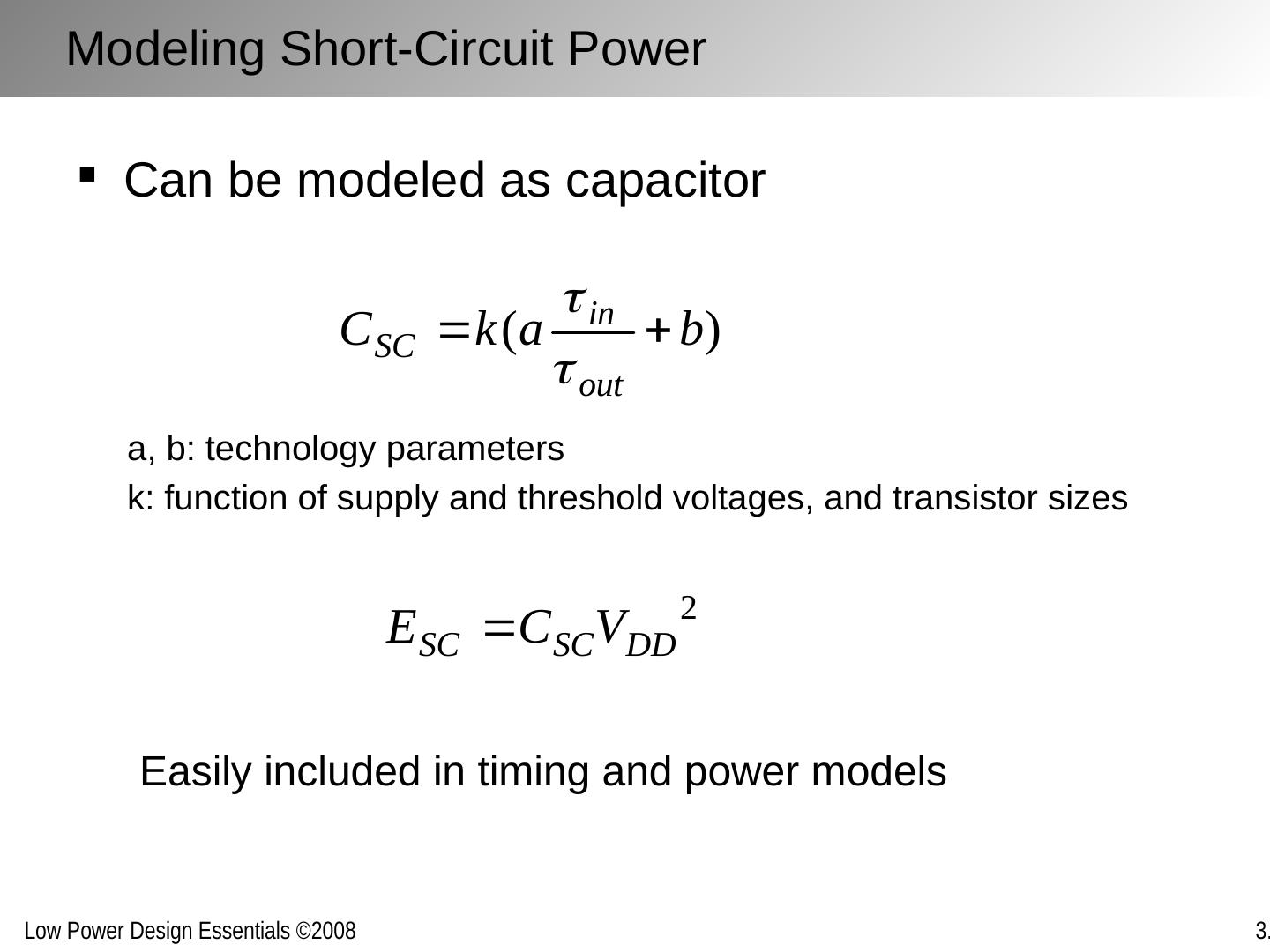
27 .Modeling Short-Circuit Power Can be modeled as capacitor a, b: technology parameters k: function of supply and threshold voltages, and transistor sizes Easily included in timing and power models
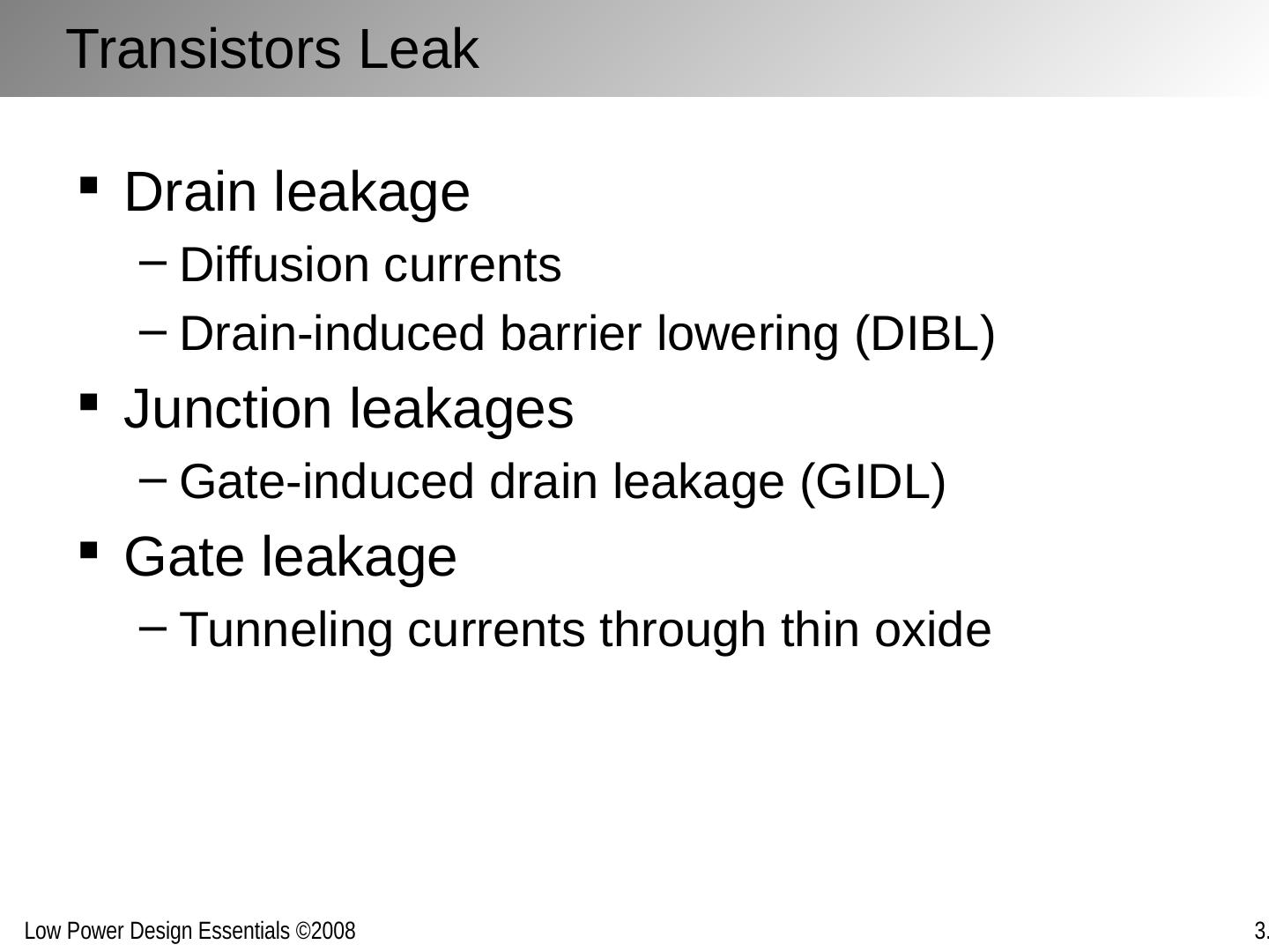
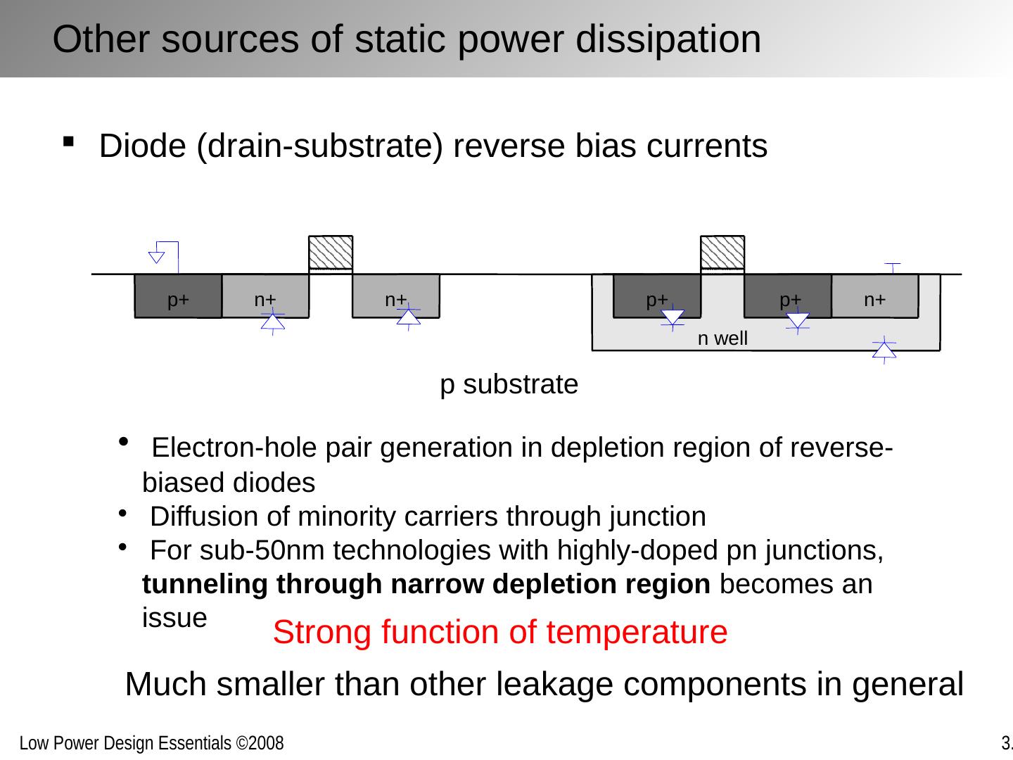
28 .Transistors Leak Drain leakage Diffusion currents Drain-induced barrier lowering (DIBL) Junction leakages Gate-induced drain leakage (GIDL) Gate leakage Tunneling currents through thin oxide
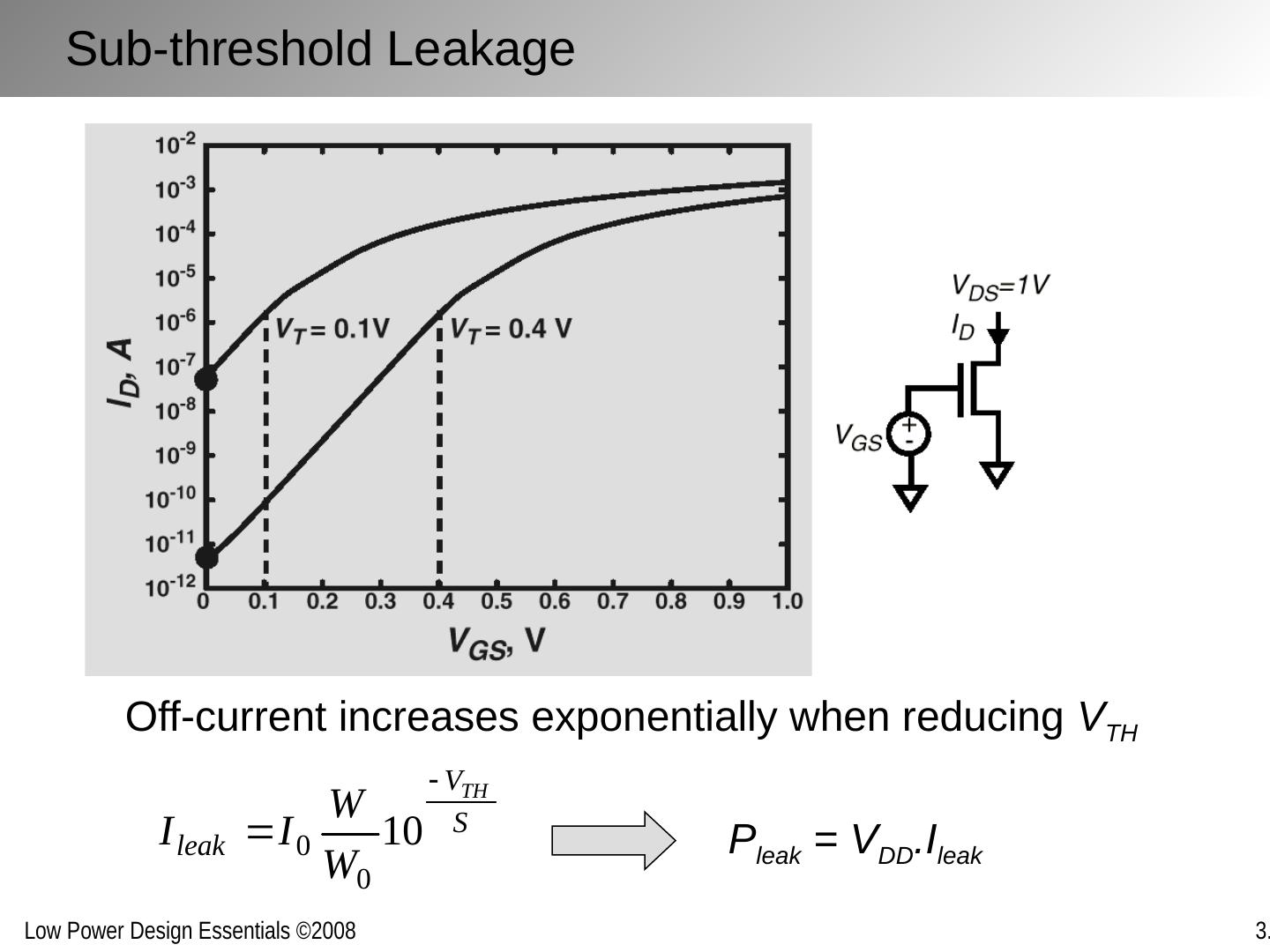
29 .Sub-threshold Leakage Off-current increases exponentially when reducing V TH P leak = V DD .I leak


