- 快召唤伙伴们来围观吧
- 微博 QQ QQ空间 贴吧
- 文档嵌入链接
- 复制
- 微信扫一扫分享
- 已成功复制到剪贴板
长沟道金属氧化物晶体
展开查看详情
1 . Lecture #25 • Design Project: – Due in class (5 PM) on Thursday May 1st • 20 pt penalty for late submissions, accepted until 5 PM on 5/8 – Your BJT design does not need to meet the performance specifications when WB and NB are varied by +/- 10% – Equation for ∆EG assumes NE is in cm-3 and T is in K EE130 QUIZ SCORE TREND • Quiz#5 Results: 30 (undergrad.’s only) 21.6 20.5 20 18.9 N=60 17.9 17.9 10 Mean=20.5 0 Std.Dev.=3.6 Q1 Q2 Q3 Q4 Q5 Spring 2003 EE130 Lecture 25, Slide 1 OUTLINE • NMOSFET I-V • Effective mobility • Transconductance • PMOSFET I-V • Subthreshold current Spring 2003 EE130 Lecture 25, Slide 2 1
2 . Ideal MOSFET I-V Characteristics (Enhancement Mode NMOS Transistor) Saturation Linear region region Spring 2003 EE130 Lecture 25, Slide 3 Review: Qualitative Operation of the NMOSFET depletion layer The potential barrier to electron flow from the source into the channel is lowered by applying VGS> VT Electrons flow from the source to the drain by drift, when VDS>0. (IDS > 0.) The channel potential varies from VS at the source end to VD at the drain end. (The inversion layer can be Spring 2003 EE130 Lecture 25, Slide 4 modeled as a resistor.) 2
3 . When VD is increased to be equal to VG-VT, the inversion-layer charge density at the drain end of the channel equals zero, i.e. the channel becomes “pinched off” As VD is increased above VG-VT, the length ∆L of the “pinch-off” region increases. The voltage applied across the inversion layer is always VDsat=VGS-VT, and so the current saturates: I Dsat = I DS V DS =VDsat If ∆L is significant compared to L, then IDS will increase slightly with increasing VDS>VDsat, due to “channel-length modulation” Spring 2003 EE130 Lecture 25, Slide 5 NMOSFET I-V Characteristics • VD > VS • Current in the channel flows by drift • Channel voltage VC(y) varies continuously between the source and the drain 2qN Aε Si ( 2ψ B + VCB ( y )) VT = VFB + VC ( y ) + 2ψ B + Cox • Channel inversion charge Q ( y) Qinv ( y ) = −Coxe VG − VFB − VC ( y ) − 2ψ B − dep Coxe W Spring 2003 EE130 Lecture 25, Slide 6 3
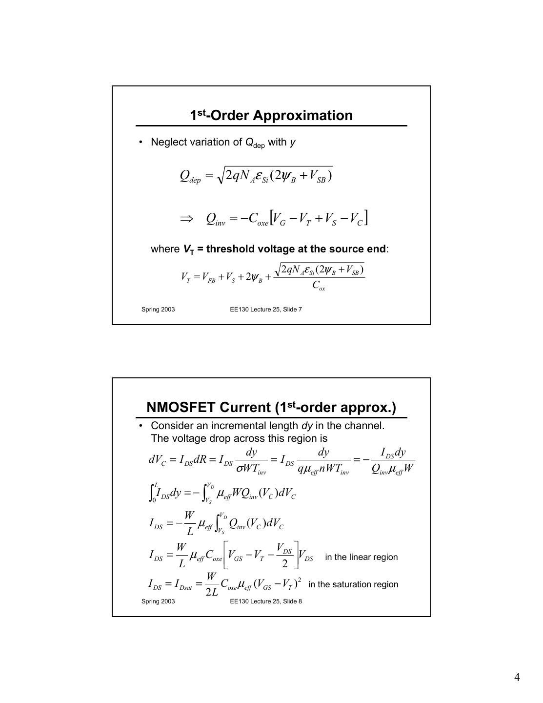
4 . 1st-Order Approximation • Neglect variation of Qdep with y Qdep = 2qN Aε Si (2ψ B + VSB ) ⇒ Qinv = −Coxe [VG − VT + VS − VC ] where VT = threshold voltage at the source end: 2qN Aε Si ( 2ψ B + VSB ) VT = VFB + VS + 2ψ B + Cox Spring 2003 EE130 Lecture 25, Slide 7 NMOSFET Current (1st-order approx.) • Consider an incremental length dy in the channel. The voltage drop across this region is dy dy I dy dVC = I DS dR = I DS = I DS = − DS σWTinv qµeff nWTinv Qinv µeff W L VD ∫I 0 DS dy = − ∫ µeff WQinv (VC )dVC VS W VD I DS = − µeff ∫ Qinv (VC )dVC L VS W V I DS = µeff Coxe VGS − VT − DS VDS in the linear region L 2 W I DS = I Dsat = Coxe µeff (VGS − VT ) 2 in the saturation region 2L Spring 2003 EE130 Lecture 25, Slide 8 4
5 . Effective Mobility V I DS = WQinv v = WQ inv µeff E = WQ inv µeff DS L = (W / L) µeff Coxe (VG − VT )VDS where µeff is the effective electron mobility The NMOSFET can be modelled as a resistor at low VDS: VDS L RDS = = I DS Wµeff Coxe (VG − VT ) Spring 2003 EE130 Lecture 25, Slide 9 µeff vs. Effective Normal Field (Vgs + V t + 0.2)/6Toxe (MV/cm) (NFET) Scattering mechanisms: • coulombic scattering • phonon scattering • surface roughness scattering (PFET) –(Vgs + 1.5V t – 0.25)/6Tox e (MV/cm) Spring 2003 EE130 Lecture 25, Slide 10 5
6 . The “Body Effect” VT is a function of VSB: VT = VT 0 + 2qN Aε Si Coxe ( 2ψ B + VSB − 2ψ B ) = VT 0 + γ ( 2ψ B + VSB − 2ψ B ) where γ is the body effect parameter When the source-body pn junction is reverse-biased, |VT| increases. Usually, we want to minimize γ so that IDsat ∝|VGS – VT| will be the same for all transistors in a circuit Spring 2003 EE130 Lecture 25, Slide 11 Problem with the “Square Law Theory” • Assumes that gate charge is purely balanced by inversion charge • Ignores variation in depletion width with distance y Spring 2003 EE130 Lecture 25, Slide 12 6
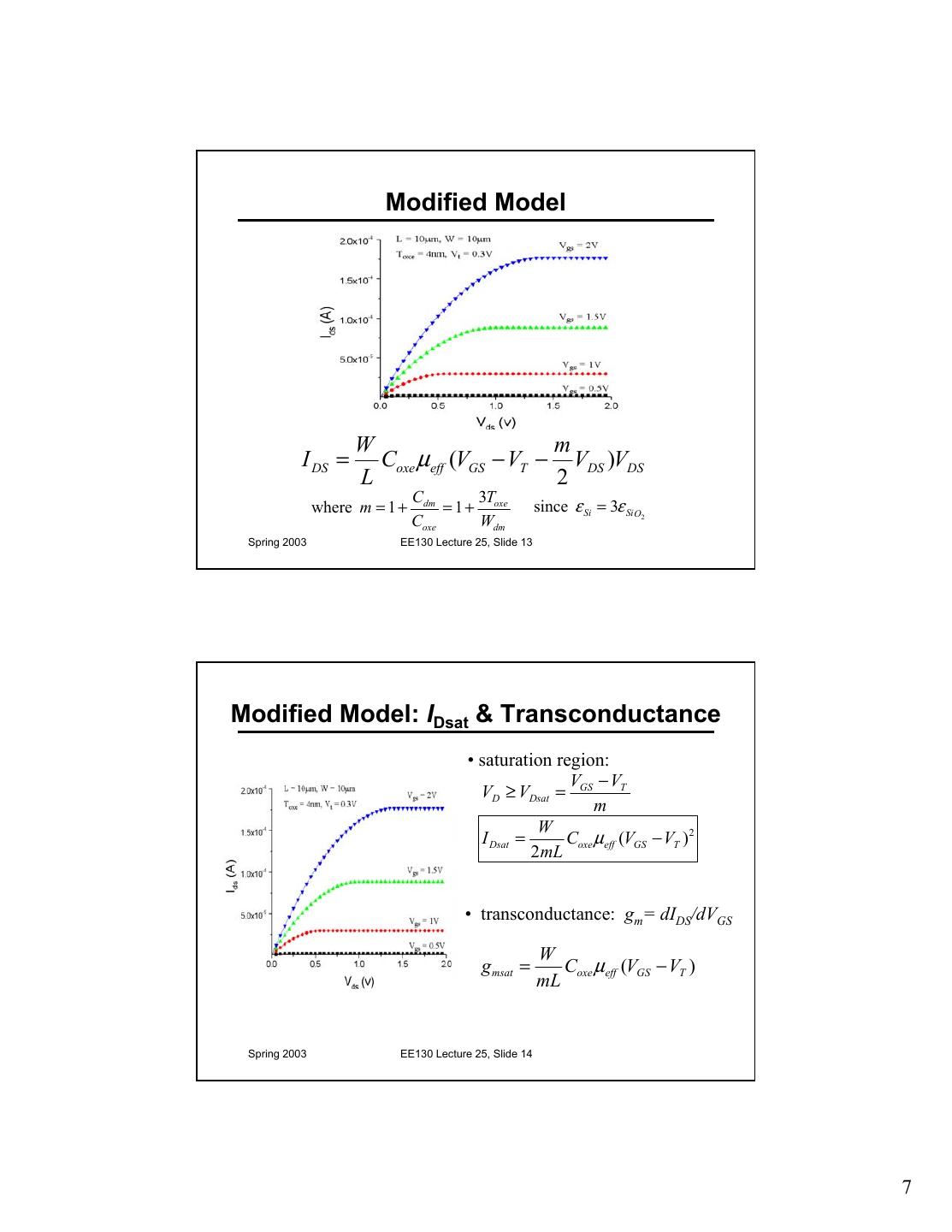
7 . Modified Model W m I DS = Coxe µeff (VGS − VT − VDS )VDS L 2 Cdm 3T where m = 1 + = 1 + oxe since ε Si = 3ε Si O2 Coxe Wdm Spring 2003 EE130 Lecture 25, Slide 13 Modified Model: IDsat & Transconductance • saturation region: V − VT VD ≥ VDsat = GS m W I Dsat = Coxe µeff (VGS − VT )2 2mL • transconductance: gm= dIDS/dVGS W g msat = Coxe µ eff (VGS − VT ) mL Spring 2003 EE130 Lecture 25, Slide 14 7
8 . MOSFET VT Measurement • VT can be determined by plotting IDS vs. VGS, using a low value of VDS Spring 2003 EE130 Lecture 25, Slide 15 P-Channel MOSFET • The PMOSFET turns on when VGS < VTp – Holes flow from SOURCE to DRAIN ⇒ DRAIN is biased at a lower potential than the SOURCE VG • VDS < 0 VS VD GATE IDS • IDS < 0 P+ P+ • |IDS| increases with N • |VGS - VTp| • |VDS| (linear region) VB • In CMOS technology, the threshold voltages are usually symmetric: VTp = -VTn Spring 2003 EE130 Lecture 25, Slide 16 8
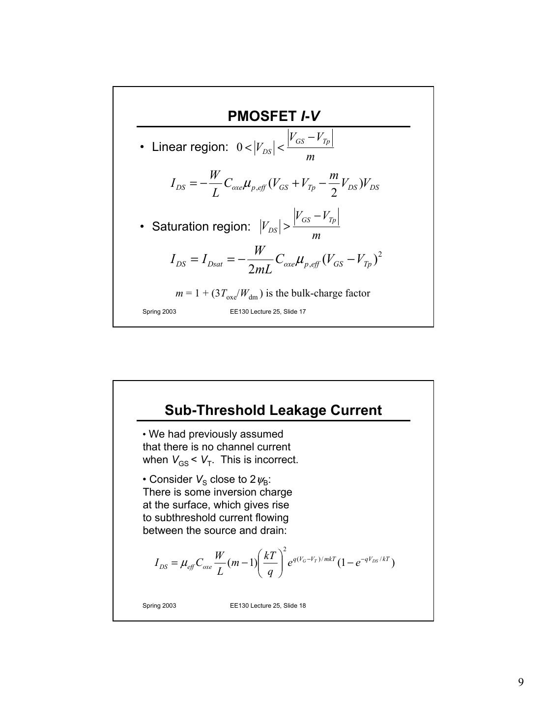
9 . PMOSFET I-V VGS − VTp • Linear region: 0 < VDS < m W m I DS = − Coxe µ p ,eff (VGS + VTp − VDS )VDS L 2 VGS − VTp • Saturation region: VDS > m W I DS = I Dsat = − Coxe µ p ,eff (VGS − VTp ) 2 2mL m = 1 + (3Toxe/Wdm ) is the bulk-charge factor Spring 2003 EE130 Lecture 25, Slide 17 Sub-Threshold Leakage Current • We had previously assumed that there is no channel current when VGS < VT. This is incorrect. • Consider VS close to 2ψB: There is some inversion charge at the surface, which gives rise to subthreshold current flowing between the source and drain: 2 W kT q (VG −VT ) / mkT I DS = µeff Coxe ( m − 1) e (1 − e − qVDS / kT ) L q Spring 2003 EE130 Lecture 25, Slide 18 9
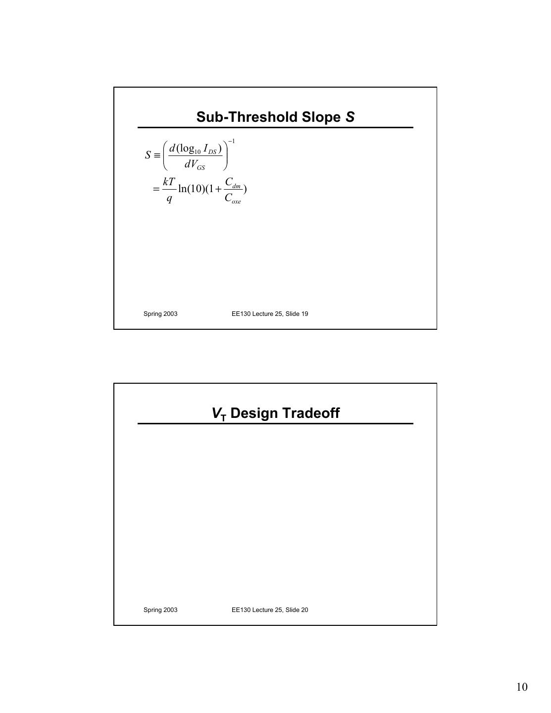
10 . Sub-Threshold Slope S −1 d (log10 I DS ) S ≡ dV GS kT C = ln(10)(1 + dm ) q Coxe Spring 2003 EE130 Lecture 25, Slide 19 VT Design Tradeoff Spring 2003 EE130 Lecture 25, Slide 20 10


