- 快召唤伙伴们来围观吧
- 微博 QQ QQ空间 贴吧
- 文档嵌入链接
- 复制
- 微信扫一扫分享
- 已成功复制到剪贴板
理想二极管与结构击穿
展开查看详情
1 . Lecture #11 OUTLINE • pn Junctions – reverse breakdown – ideal diode analysis » current flow (qualitative) » minority carrier distributions Reading: Chapter 6 Spring 2003 EE130 Lecture 11, Slide 1 A Note of Caution • Typically, pn junctions in IC devices are formed by counter-doping. The equations derived in class (and in the textbook) can be readily applied to such diodes if NA ≡ net acceptor doping on p-side (NA-ND)p-side ND ≡ net donor doping on n-side (ND-NA)n-side Spring 2003 EE130 Lecture 11, Slide 2 1
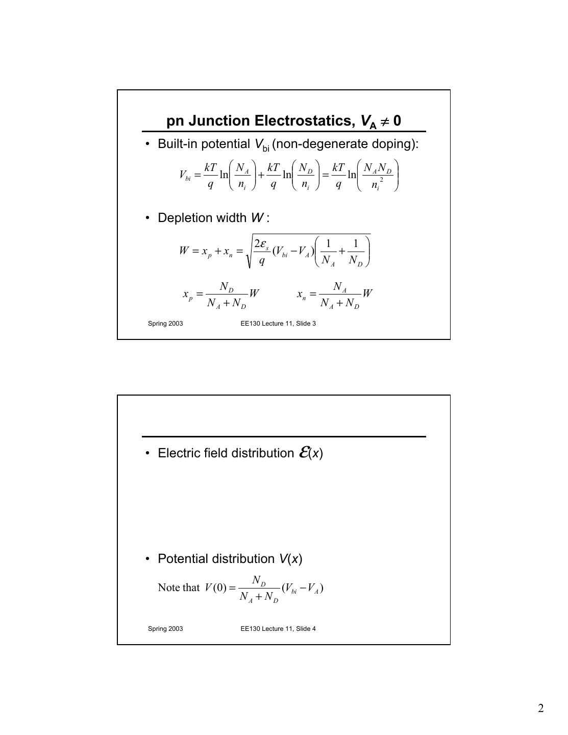
2 . pn Junction Electrostatics, VA ≠ 0 • Built-in potential Vbi (non-degenerate doping): kT N A kT N D kT N A N D Vbi = ln + ln = ln q ni q ni q ni 2 • Depletion width W : 2ε s 1 1 W = x p + xn = (Vbi − V A ) + q N A ND ND NA xp = W xn = W N A + ND N A + ND Spring 2003 EE130 Lecture 11, Slide 3 • Electric field distribution ε(x) • Potential distribution V(x) ND Note that V (0) = (Vbi − V A ) N A + ND Spring 2003 EE130 Lecture 11, Slide 4 2
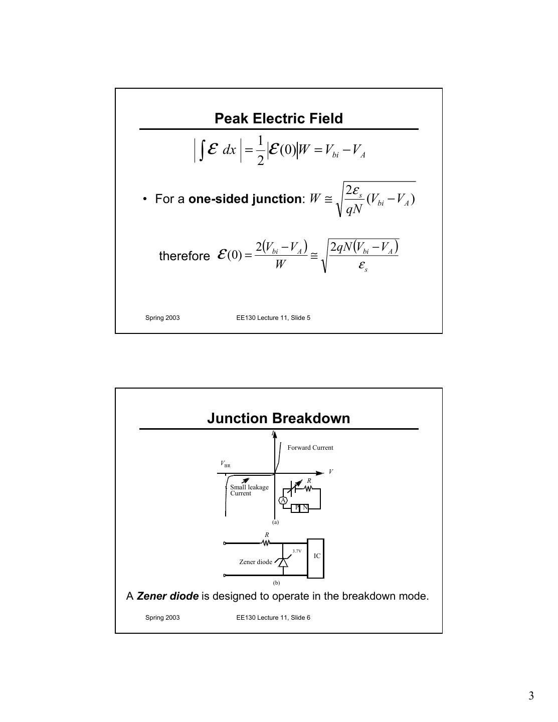
3 . Peak Electric Field ∫ ε dx = 1 2 ε (0) W = Vbi − VA 2ε s • For a one-sided junction: W ≅ (Vbi − VA ) qN therefore ε (0) = 2(V W− V ) ≅bi A 2qN (Vbi − VA ) εs Spring 2003 EE130 Lecture 11, Slide 5 Junction Breakdown I Forward Current VBR V R Small leakage Current A P N (a) R 3.7V IC Zener diode (b) A Zener diode is designed to operate in the breakdown mode. Spring 2003 EE130 Lecture 11, Slide 6 3
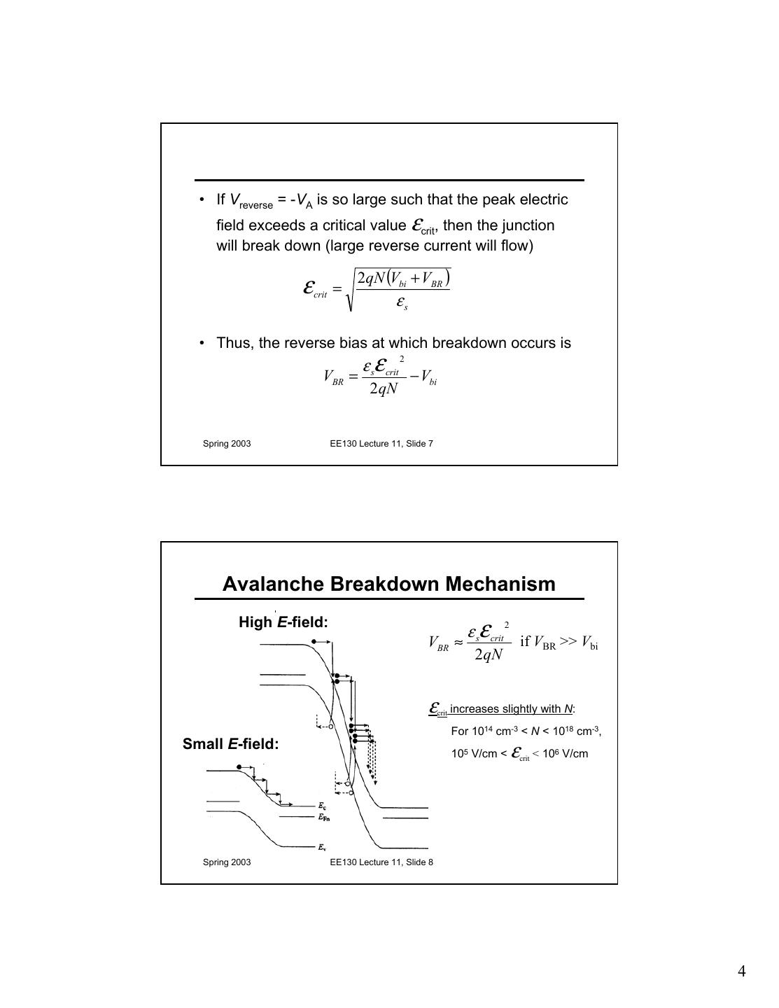
4 . • If Vreverse = -VA is so large such that the peak electric field exceeds a critical value εcrit, then the junction will break down (large reverse current will flow) 2qN (Vbi + VBR ) ε crit = εs • Thus, the reverse bias at which breakdown occurs is ε sε crit 2 VBR = − Vbi 2qN Spring 2003 EE130 Lecture 11, Slide 7 Avalanche Breakdown Mechanism ε sε crit High E-field: 2 VBR ≈ if VBR >> Vbi 2qN ε crit increases slightly with N: For 1014 cm-3 < N < 1018 cm-3, Small E-field: 105 V/cm < ε crit < 106 V/cm Spring 2003 EE130 Lecture 11, Slide 8 4
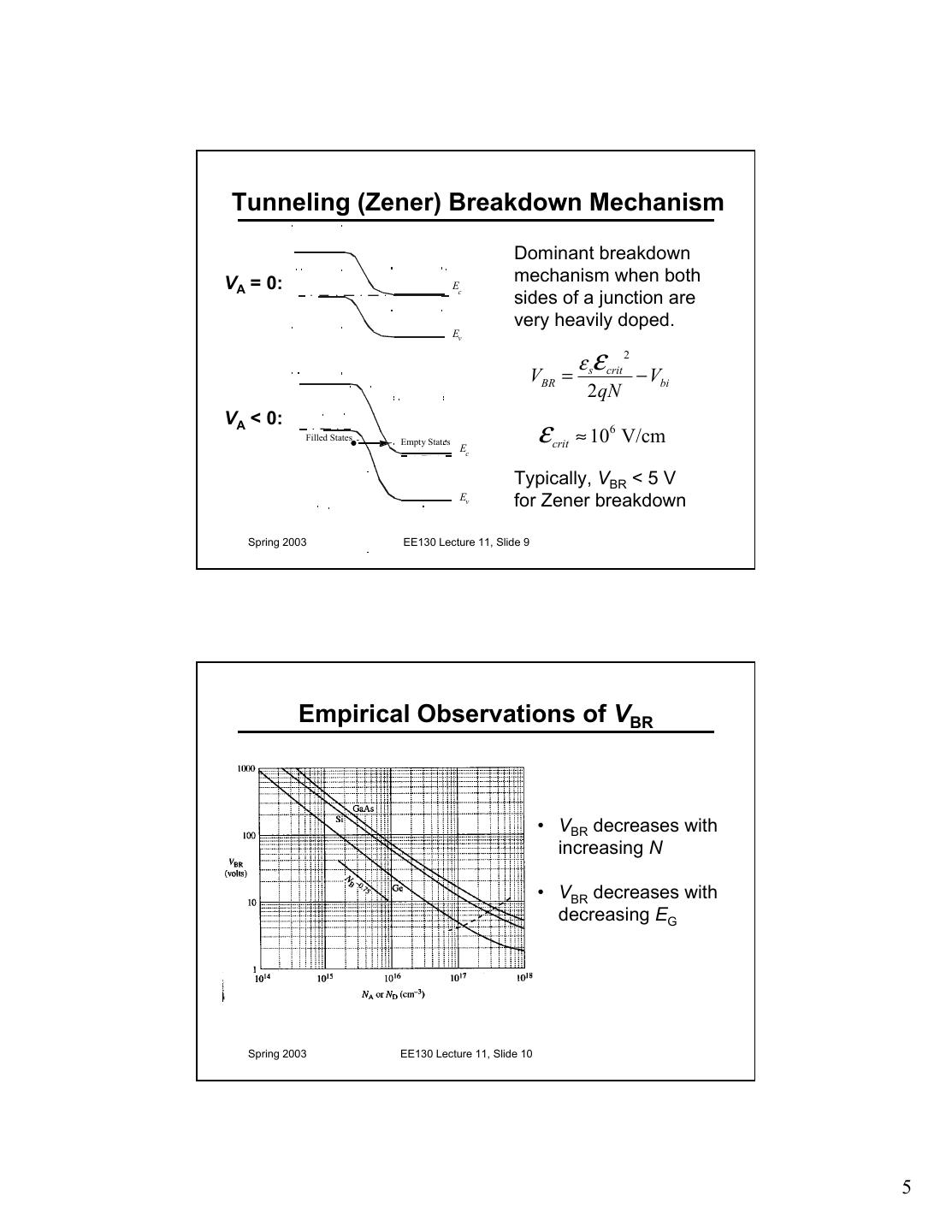
5 .Tunneling (Zener) Breakdown Mechanism Dominant breakdown VA = 0: Ec mechanism when both sides of a junction are very heavily doped. Ev ε sε crit 2 VBR = − Vbi 2qN VA < 0: Filled States - Empty States Ec ε crit ≈ 106 V/cm Typically, VBR < 5 V Ev for Zener breakdown Spring 2003 EE130 Lecture 11, Slide 9 Empirical Observations of VBR • VBR decreases with increasing N • VBR decreases with decreasing EG Spring 2003 EE130 Lecture 11, Slide 10 5
6 . Breakdown Temperature Dependence • For the avalanche mechanism: VBR increases with increasing T – Mean free path decreases • For the tunneling mechanism: VBR decreases with increasing T – Flux of valence-band electrons available for tunneling increases Spring 2003 EE130 Lecture 11, Slide 11 Current Flow in a pn Junction Diode • When a forward bias (VA>0) is applied, the potential barrier to diffusion across the junction is reduced – Minority carriers are “injected” into the quasi- neutral regions => ∆np > 0, ∆pn > 0 • Minority carriers diffuse in the quasi-neutral regions, recombining with majority carriers Spring 2003 EE130 Lecture 11, Slide 12 6
7 . • Current density J = Jn(x) + Jp(x) d ( ∆n ) J n ( x ) = qµn nε + qDn = qµn nε + qDn dn dx dx d ( ∆p ) J p ( x ) = qµ p pε = qµ p pε − qD p dp − qD p dx dx • J is constant throughout the diode, but Jn(x) and Jp(x) vary with position Spring 2003 EE130 Lecture 11, Slide 13 Ideal Diode Analysis: Assumptions • Non-degenerately doped step junction • Steady-state conditions • Low-level injection conditions prevail in the quasi-neutral regions • Recombination-generation is negligible in the depletion region dJ n dJ p ⇒ = 0, =0 dx dx i.e. Jn & Jp are constant inside the depletion region Spring 2003 EE130 Lecture 11, Slide 14 7
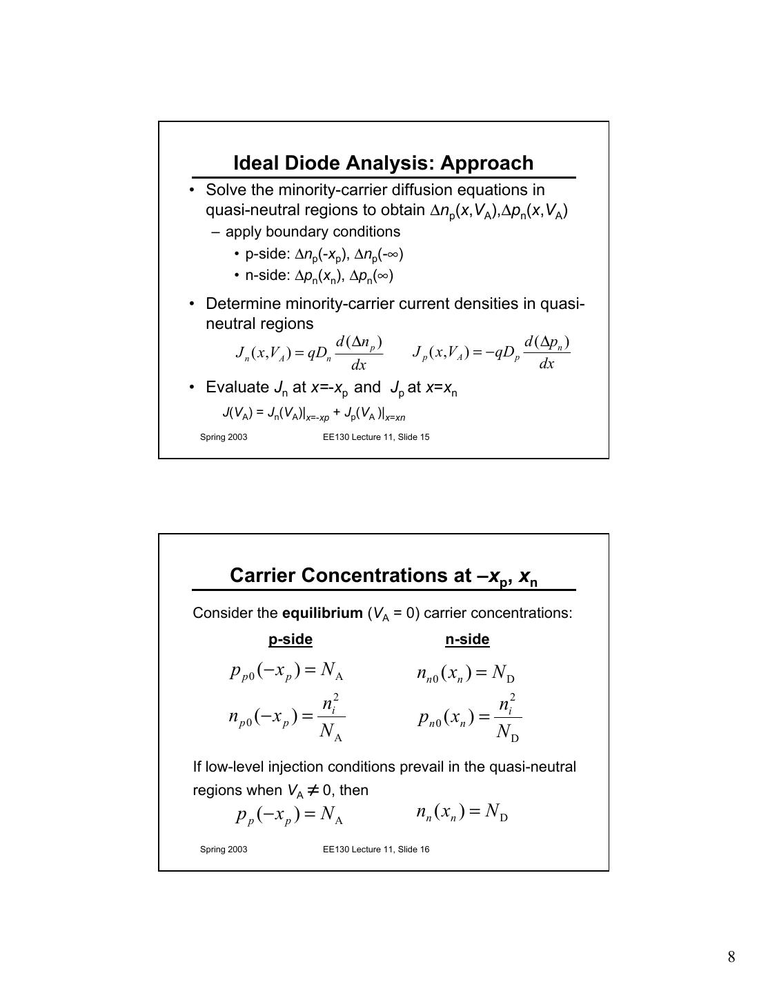
8 . Ideal Diode Analysis: Approach • Solve the minority-carrier diffusion equations in quasi-neutral regions to obtain ∆np(x,VA),∆pn(x,VA) – apply boundary conditions • p-side: ∆np(-xp), ∆np(-∞) • n-side: ∆pn(xn), ∆pn(∞) • Determine minority-carrier current densities in quasi- neutral regions d ( ∆n p ) d ( ∆pn ) J n ( x,VA ) = qDn J p ( x,VA ) = − qD p dx dx • Evaluate Jn at x=-xp and Jp at x=xn J(VA) = Jn(VA)|x=-xp + Jp(VA )|x=xn Spring 2003 EE130 Lecture 11, Slide 15 Carrier Concentrations at –xp, xn Consider the equilibrium (VA = 0) carrier concentrations: p-side n-side p p 0 (− x p ) = N A nn 0 ( xn ) = N D ni2 ni2 n p 0 (− x p ) = p n 0 ( xn ) = NA ND If low-level injection conditions prevail in the quasi-neutral regions when VA ≠ 0, then p p (− x p ) = N A nn ( xn ) = N D Spring 2003 EE130 Lecture 11, Slide 16 8
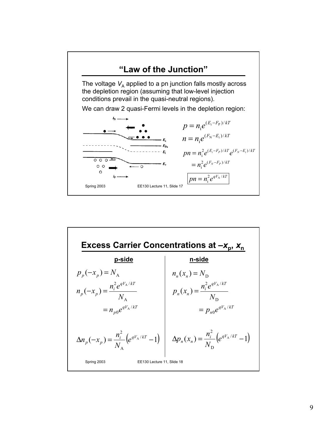
9 . “Law of the Junction” The voltage VA applied to a pn junction falls mostly across the depletion region (assuming that low-level injection conditions prevail in the quasi-neutral regions). We can draw 2 quasi-Fermi levels in the depletion region: p = ni e ( Ei − FP ) / kT n = ni e ( FN − Ei ) / kT pn = ni2e( Ei − FP ) / kT e( FN − Ei ) / kT = ni2e( FN − FP ) / kT pn = ni2e qVA / kT Spring 2003 EE130 Lecture 11, Slide 17 Excess Carrier Concentrations at –xp, xn p-side n-side p p (− x p ) = N A nn ( xn ) = N D ni2 e qVA / kT ni2 e qVA / kT n p (− x p ) = p n ( xn ) = NA ND = n p 0 e qVA / kT = pn 0 e qVA / kT ∆n p (− x p ) = e ( ni2 qVA / kT −1 ) ∆pn ( xn ) = ni2 qVA / kT ND e −1 ( ) NA Spring 2003 EE130 Lecture 11, Slide 18 9
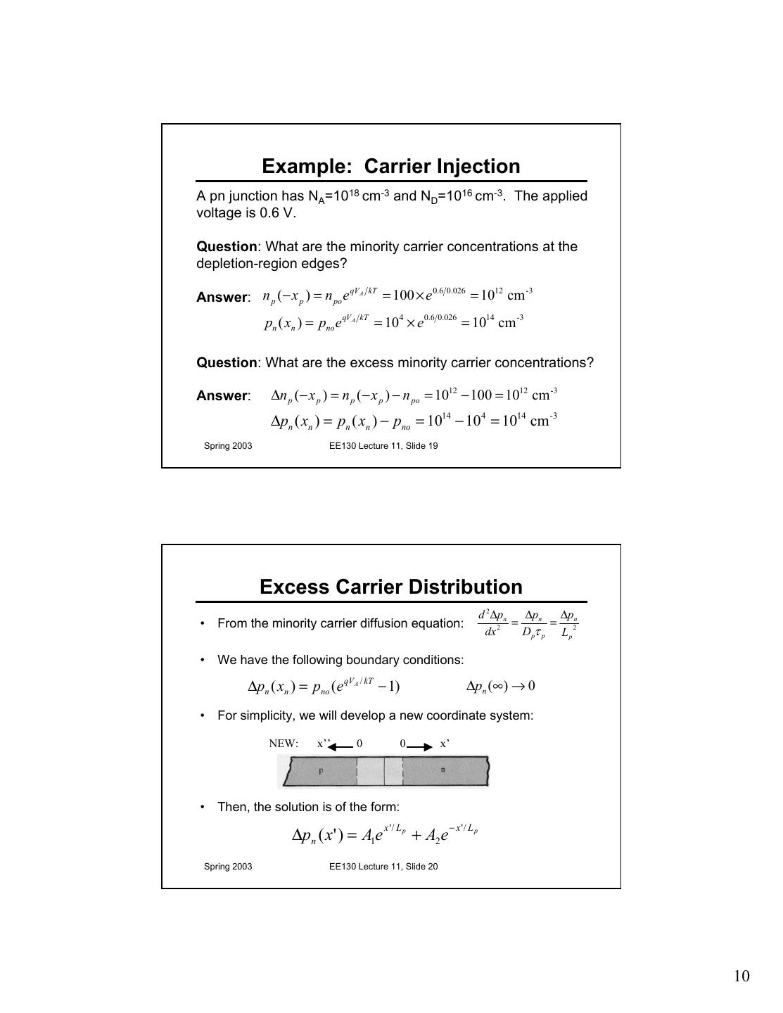
10 . Example: Carrier Injection A pn junction has NA=1018 cm-3 and ND=1016 cm-3. The applied voltage is 0.6 V. Question: What are the minority carrier concentrations at the depletion-region edges? Answer: n p (− x p ) = n po e A = 100 × e 0.6 0.026 = 1012 cm -3 qV kT pn ( xn ) = pno e qVA kT = 104 × e0.6 0.026 = 1014 cm -3 Question: What are the excess minority carrier concentrations? Answer: ∆n p (− x p ) = n p ( − x p ) − n po = 1012 − 100 = 1012 cm -3 ∆pn ( xn ) = pn ( xn ) − pno = 1014 − 104 = 1014 cm -3 Spring 2003 EE130 Lecture 11, Slide 19 Excess Carrier Distribution d 2 ∆pn ∆pn ∆p • From the minority carrier diffusion equation: = = 2n dx 2 D pτ p L p • We have the following boundary conditions: ∆pn ( xn ) = pno ( e qVA / kT − 1) ∆pn (∞) → 0 • For simplicity, we will develop a new coordinate system: NEW: x’’ 0 0 x’ • Then, the solution is of the form: x '/ L p − x '/ L p ∆pn ( x' ) = A1e + A2 e Spring 2003 EE130 Lecture 11, Slide 20 10
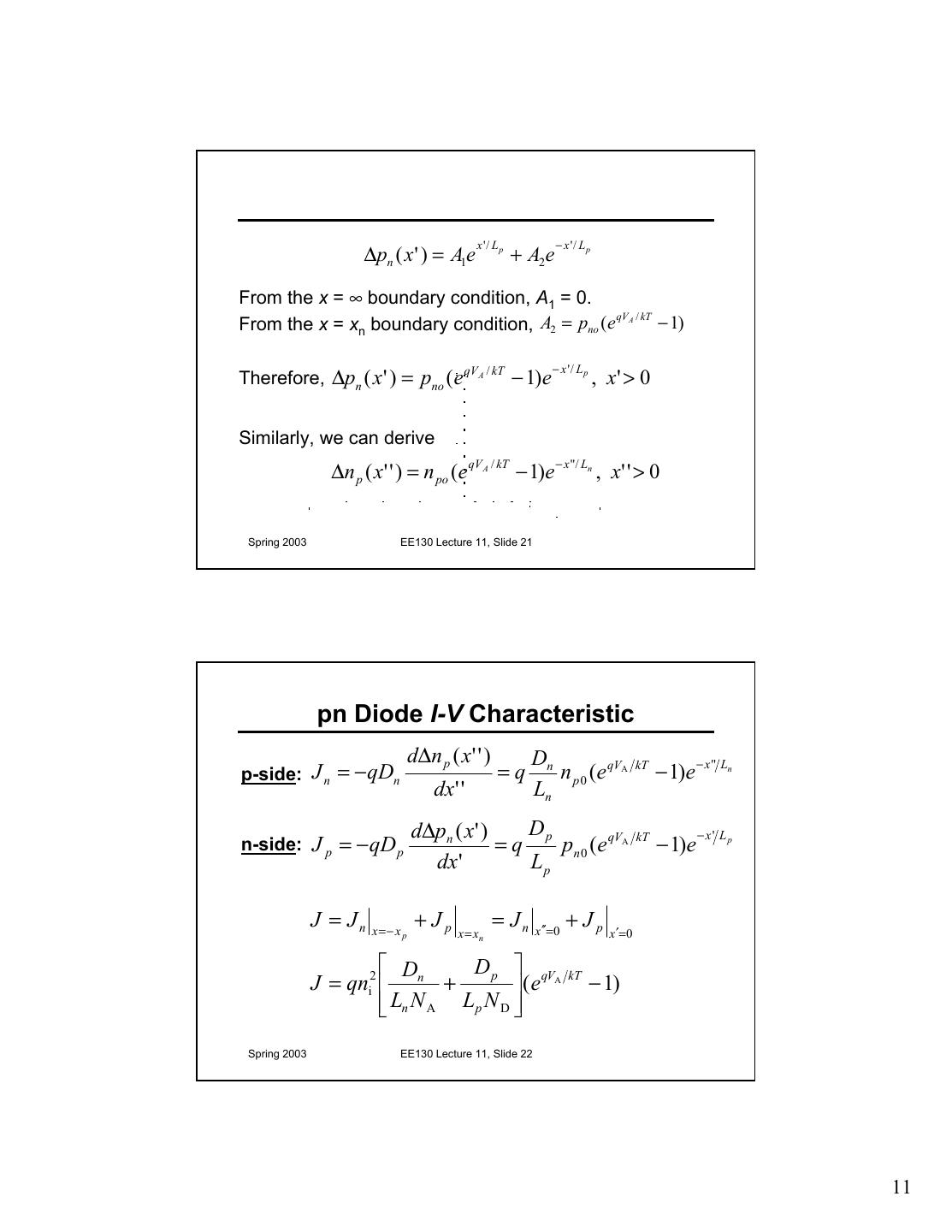
11 . x '/ Lp − x '/ Lp ∆pn ( x ' ) = A1e + A2e From the x = ∞ boundary condition, A1 = 0. From the x = xn boundary condition, A2 = pno ( e A − 1) qV / kT − x '/ Lp Therefore, ∆pn ( x ' ) = pno ( e qVA / kT − 1)e , x' > 0 Similarly, we can derive ∆n p ( x' ' ) = n po (e qV A / kT − 1)e − x ''/ Ln , x' ' > 0 Spring 2003 EE130 Lecture 11, Slide 21 pn Diode I-V Characteristic d∆n p ( x' ' ) Dn p-side: J n = − qDn =q n p 0 (e qVA kT − 1)e − x '' Ln dx ' ' Ln d∆pn ( x' ) Dp −x' Lp n-side: J p = − qD p =q pn 0 (e qVA kT − 1)e dx' Lp J = Jn x=− x p + Jp = Jn x ′′=0 + Jp x = xn x ′= 0 D D p qVA J = qni2 n + ( e kT − 1) Ln N A Lp N D Spring 2003 EE130 Lecture 11, Slide 22 11
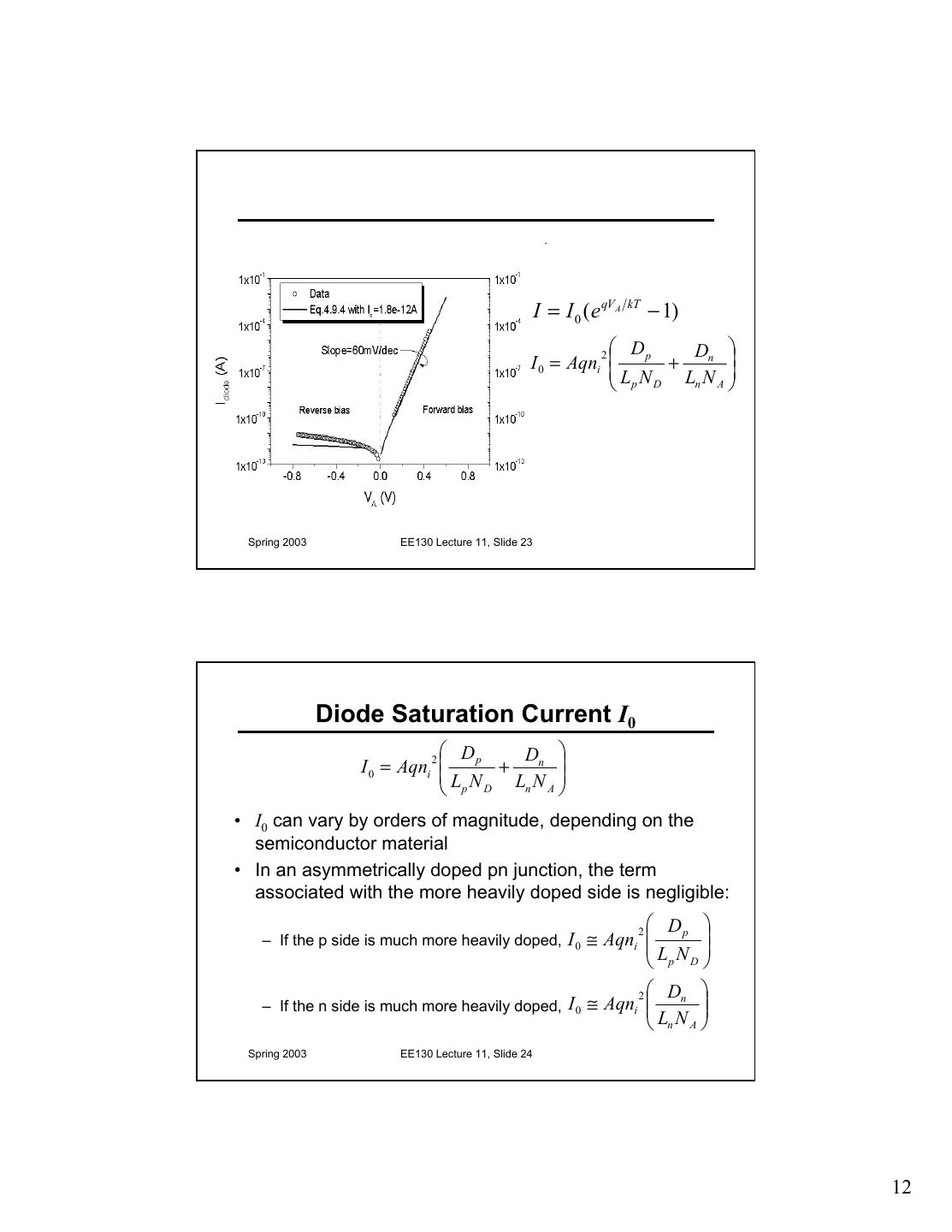
12 . I = I 0 ( e qVA kT − 1) 2 Dp Dn I 0 = Aqni + L N p D Ln N A Spring 2003 EE130 Lecture 11, Slide 23 Diode Saturation Current I0 2 Dp Dn I 0 = Aqni + L N p D Ln N A • I0 can vary by orders of magnitude, depending on the semiconductor material • In an asymmetrically doped pn junction, the term associated with the more heavily doped side is negligible: 2 Dp – If the p side is much more heavily doped, I 0 ≅ Aqni L N p D 2 D – If the n side is much more heavily doped, I 0 ≅ Aqni n Ln N A Spring 2003 EE130 Lecture 11, Slide 24 12


