- 快召唤伙伴们来围观吧
- 微博 QQ QQ空间 贴吧
- 文档嵌入链接
- 复制
- 微信扫一扫分享
- 已成功复制到剪贴板
静电学、能带图
展开查看详情
1 . Lecture #21 OUTLINE The MOS Capacitor • Electrostatics Reading: Course Reader Spring 2003 EE130 Lecture 21, Slide 1 MOS Capacitor Structure • Typical MOS capacitors and MOS capacitor (cross-sectional view) transistors in ICs today employ – heavily doped polycrystalline Si (“poly-Si”) film as the gate- electrode material GATE • n+-type, for “n-channel” xox transistors (NMOS) • p+-type, for “p-channel” VG +_ transistors (PMOS) – SiO2 as the gate dielectric Si • band gap = 9 eV • εr,SiO2 = 3.9 – Si as the semiconductor material • p-type, for “n-channel” transistors (NMOS) • n-type, for “p-channel” transistors (PMOS) Spring 2003 EE130 Lecture 21, Slide 2 1
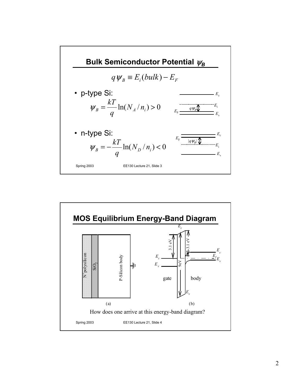
2 . Bulk Semiconductor Potential ψB qψ B ≡ Ei (bulk ) − E F • p-type Si: Ec kT ψB = ln( N A / ni ) > 0 EF qψ B Ei q Ev • n-type Si: EF Ec kT |qψB| ψ B = − ln( N D / ni ) < 0 Ei q Ev Spring 2003 EE130 Lecture 21, Slide 3 MOS Equilibrium Energy-Band Diagram Ec 3.1 eV 3.1 eV Ec Ef N +polysilicon Ec P-Silicon body Ev 9eV Ev SiO2 gate body Ev (a) (b) How does one arrive at this energy-band diagram? Spring 2003 EE130 Lecture 21, Slide 4 2
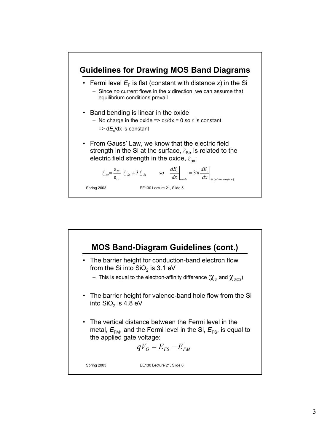
3 .Guidelines for Drawing MOS Band Diagrams • Fermi level EF is flat (constant with distance x) in the Si – Since no current flows in the x direction, we can assume that equilibrium conditions prevail • Band bending is linear in the oxide – No charge in the oxide => d /dx = 0 so is constant => dEc/dx is constant • From Gauss’ Law, we know that the electric field strength in the Si at the surface, Si, is related to the electric field strength in the oxide, ox: ε Si dEc dEc ox = Si ≅3 Si so = 3× ε ox dx oxide dx Si ( at the surface ) Spring 2003 EE130 Lecture 21, Slide 5 MOS Band-Diagram Guidelines (cont.) • The barrier height for conduction-band electron flow from the Si into SiO2 is 3.1 eV – This is equal to the electron-affinity difference (χSi and χSiO2) • The barrier height for valence-band hole flow from the Si into SiO2 is 4.8 eV • The vertical distance between the Fermi level in the metal, EFM, and the Fermi level in the Si, EFS, is equal to the applied gate voltage: qVG = E FS − E FM Spring 2003 EE130 Lecture 21, Slide 6 3
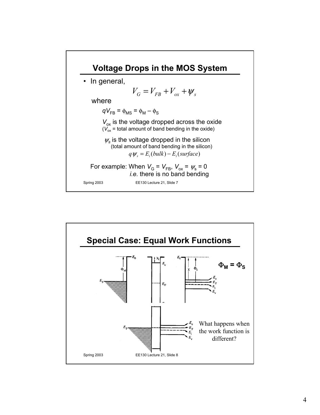
4 . Voltage Drops in the MOS System • In general, VG = VFB + Vox + ψ s where qVFB = φMS = φM – φS Vox is the voltage dropped across the oxide (Vox = total amount of band bending in the oxide) ψs is the voltage dropped in the silicon (total amount of band bending in the silicon) qψ s = Ei (bulk ) − Ei ( surface) For example: When VG = VFB, Vox = ψs = 0 i.e. there is no band bending Spring 2003 EE130 Lecture 21, Slide 7 Special Case: Equal Work Functions ΦM = ΦS What happens when the work function is different? Spring 2003 EE130 Lecture 21, Slide 8 4
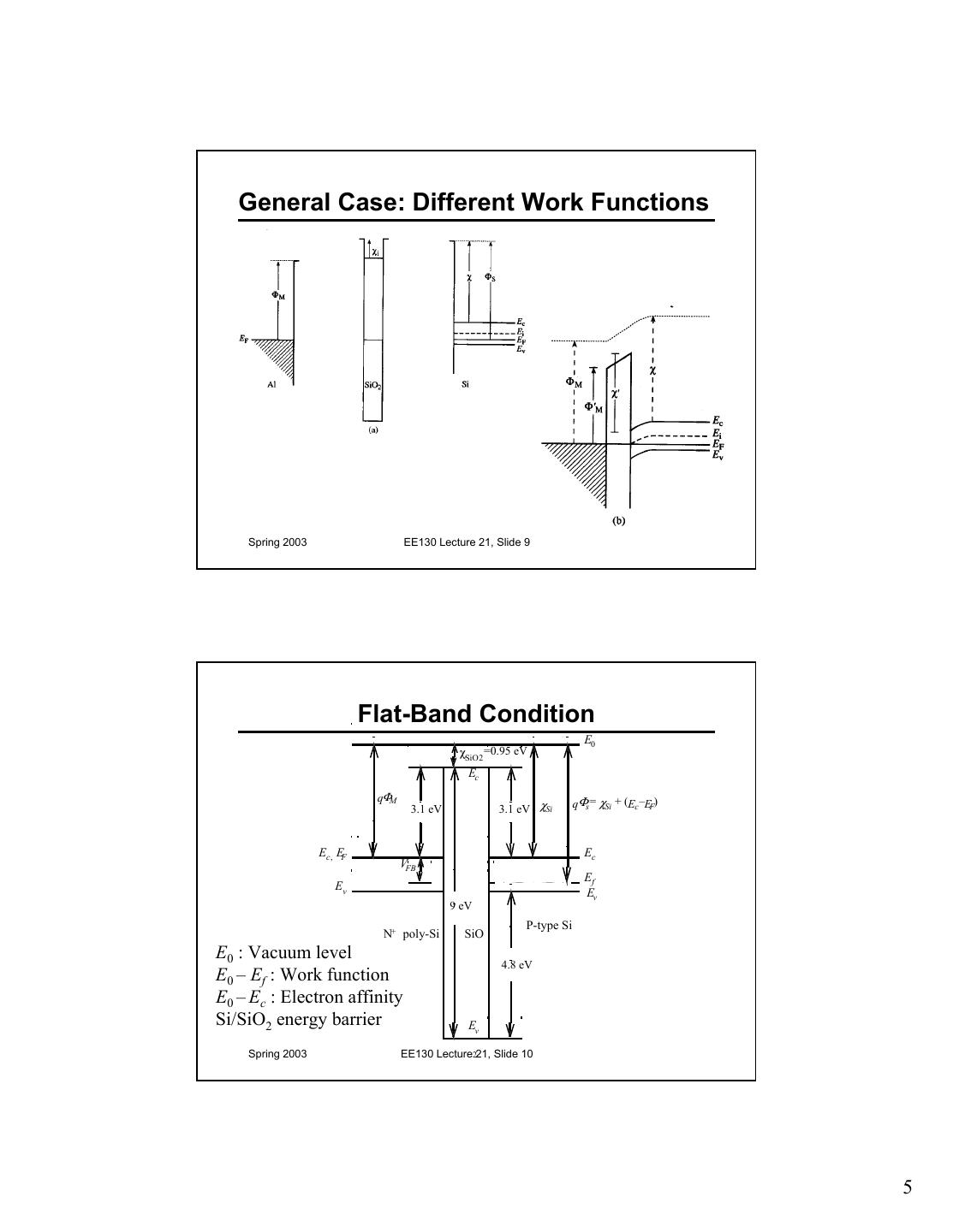
5 . General Case: Different Work Functions Spring 2003 EE130 Lecture 21, Slide 9 Flat-Band Condition E0 χSiO2 =0.95 eV Ec qΦM 3.1 eV 3.1 eV χSi qΦs = χSi + (Ec –EF) Ec, EF Ec VFB Ef Ev Ev 9 eV P-type Si N+ poly-Si SiO E0 : Vacuum level 4.8 eV E0 – Ef : Work function E0 – Ec : Electron affinity Si/SiO2 energy barrier Ev Spring 2003 EE130 Lecture221, Slide 10 5
6 . MOS Band Diagrams (n-type Si) Decrease VG (toward more negative values) -> move the gate energy-bands up, relative to the Si decrease VG decrease VG • Accumulation • Depletion • Inversion – VG > VFB – VG < VFB – VG < VT – Electrons – Electrons – Surface accumulate at repelled becomes surface from surface p-type Spring 2003 EE130 Lecture 21, Slide 11 Biasing Conditions for p-type Si increase VG increase VG VG = VFB VG < VFB VT > VG > VFB Spring 2003 EE130 Lecture 21, Slide 12 6
7 . Accumulation (n+ poly-Si gate, p-type Si) M O S VG < VFB 3.1 eV | qVox | Ec= EFM GATE Ev - - - - - - |qVG | |qψs| is small, ≈ 0 + + + + + + VG +_ Ec p-type Si 4.8 eV EFS Ev Mobile carriers (holes) accumulate at Si surface VG ≅ VFB + Vox Spring 2003 EE130 Lecture 21, Slide 13 Accumulation Layer Charge Density VG < VFB Vox ≅ VG − VFB From Gauss’ Law: ox = −Qacc / ε SiO2 GATE - - - - - - + + + + + + tox Vox = t = −Qacc / Cox ox ox + VG _ Qacc (C/cm2) where Cox ≡ ε SiO2 / tox p-type Si (units: F/cm2) ⇒ Qacc = −Cox (VG − VFB ) > 0 Spring 2003 EE130 Lecture 21, Slide 14 7
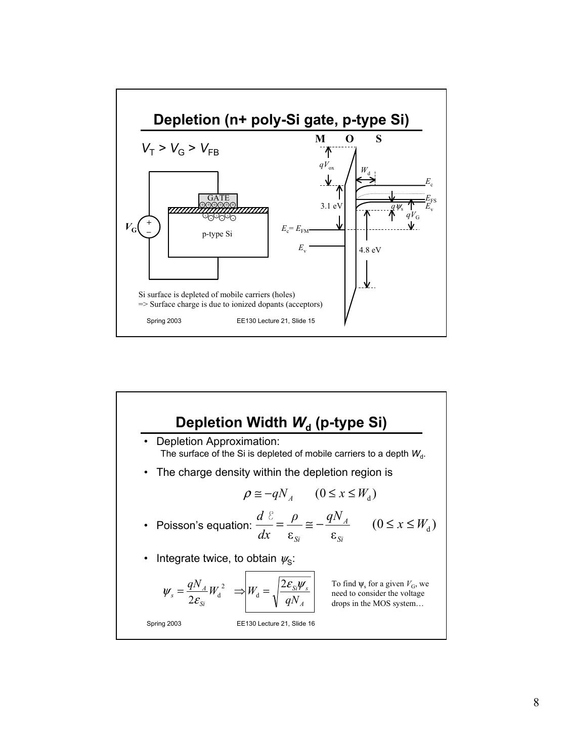
8 . Depletion (n+ poly-Si gate, p-type Si) M O S VT > VG > VFB qVox Wd Ec GATE EFS + + + + + + 3.1 eV qψ s Ev - - - - - - qVG + VG _ Ec= EFM p-type Si Ev 4.8 eV Si surface is depleted of mobile carriers (holes) => Surface charge is due to ionized dopants (acceptors) Spring 2003 EE130 Lecture 21, Slide 15 Depletion Width Wd (p-type Si) • Depletion Approximation: The surface of the Si is depleted of mobile carriers to a depth Wd. • The charge density within the depletion region is ρ ≅ − qN A (0 ≤ x ≤ Wd ) d ρ qN A • Poisson’s equation: = ≅− (0 ≤ x ≤ Wd ) dx ε Si ε Si • Integrate twice, to obtain ψS: qN A 2 2ε Siψ s To find ψs for a given VG, we ψs = Wd ⇒ Wd = need to consider the voltage 2ε Si qN A drops in the MOS system… Spring 2003 EE130 Lecture 21, Slide 16 8
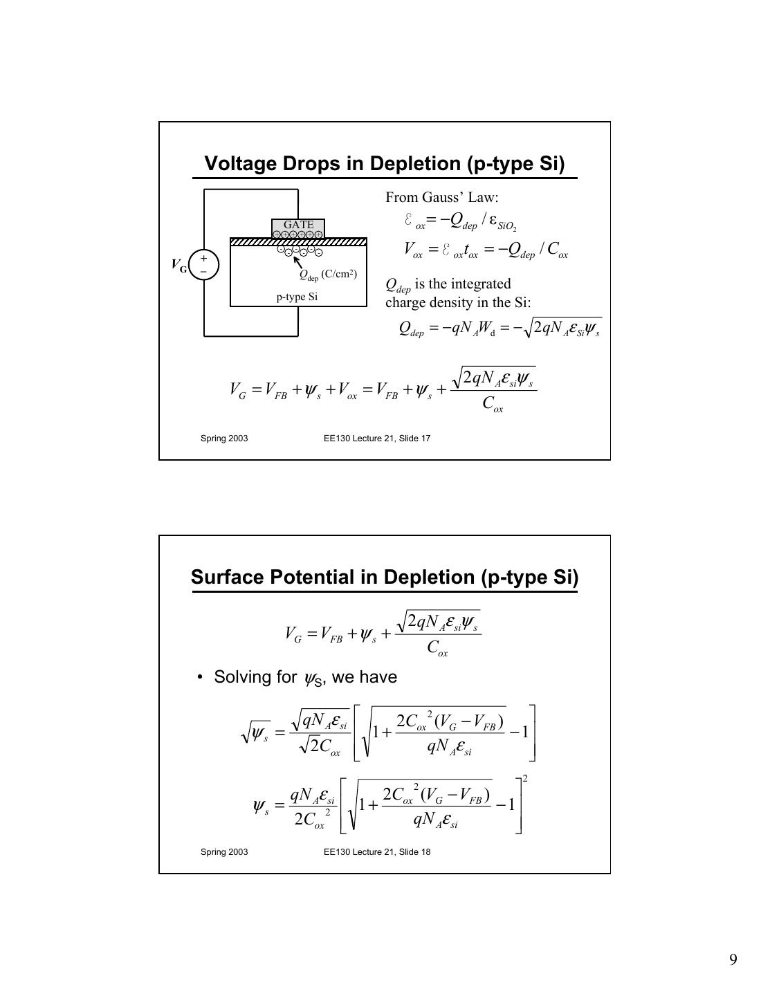
9 . Voltage Drops in Depletion (p-type Si) From Gauss’ Law: GATE ox = −Qdep / ε SiO2 + + + + + + - - - - - - Vox = t = −Qdep / Cox ox ox VG +_ Qdep (C/cm2) Qdep is the integrated p-type Si charge density in the Si: Qdep = − qN AWd = − 2qN Aε Siψ s 2 qN Aε siψ s VG = VFB + ψ s + Vox = VFB + ψ s + Cox Spring 2003 EE130 Lecture 21, Slide 17 Surface Potential in Depletion (p-type Si) 2 qN Aε siψ s VG = VFB + ψ s + Cox • Solving for ψS, we have qN Aε si 2Cox (VG − VFB ) 2 ψs = 1+ − 1 2Cox qN Aε si 2 qN Aε si 2Cox (VG − VFB ) 2 ψs = 1+ − 1 2Cox 2 qN Aε si Spring 2003 EE130 Lecture 21, Slide 18 9
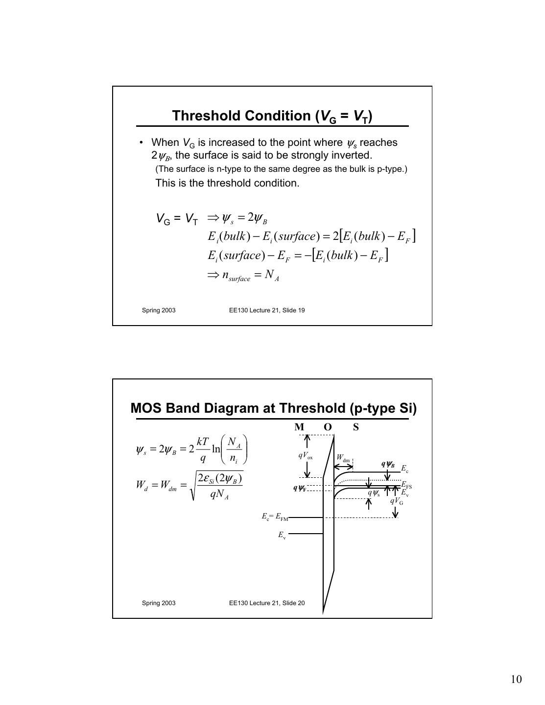
10 . Threshold Condition (VG = VT) • When VG is increased to the point where ψs reaches 2ψΒ, the surface is said to be strongly inverted. (The surface is n-type to the same degree as the bulk is p-type.) This is the threshold condition. VG = VT ⇒ ψ s = 2ψ B E i (bulk ) − Ei ( surface) = 2[Ei (bulk ) − E F ] Ei ( surface ) − EF = −[Ei (bulk ) − E F ] ⇒ nsurface = N A Spring 2003 EE130 Lecture 21, Slide 19 MOS Band Diagram at Threshold (p-type Si) M O S kT N A ψ s = 2ψ B = 2 ln q ni qVox Wdm qψ B Ec 2ε Si ( 2ψ B ) Wd = Wdm = qψ F EFS qN A qψ s Ev qVG Ec= EFM Ev Spring 2003 EE130 Lecture 21, Slide 20 10
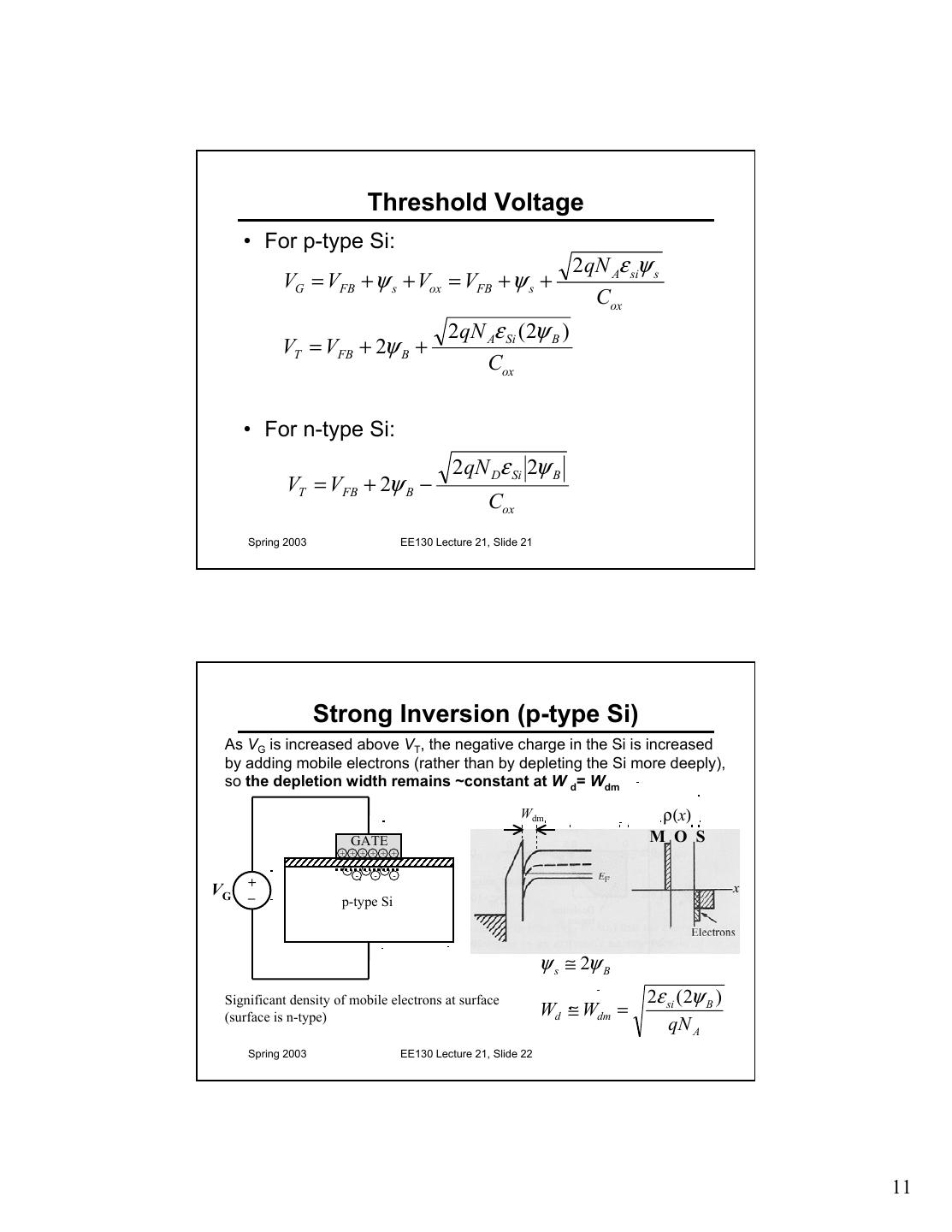
11 . Threshold Voltage • For p-type Si: 2 qN Aε siψ s VG = VFB + ψ s + Vox = VFB + ψ s + Cox 2qN Aε Si ( 2ψ B ) VT = VFB + 2ψ B + Cox • For n-type Si: 2qN Dε Si 2ψ B VT = VFB + 2ψ B − Cox Spring 2003 EE130 Lecture 21, Slide 21 Strong Inversion (p-type Si) As VG is increased above VT, the negative charge in the Si is increased by adding mobile electrons (rather than by depleting the Si more deeply), so the depletion width remains ~constant at W d= Wdm Wdm ρ(x) GATE M O S + + + + + + - - - - - - VG +_ x p-type Si ψ s ≅ 2ψ B Significant density of mobile electrons at surface 2ε si ( 2ψ B ) (surface is n-type) Wd ≅ Wdm = qN A Spring 2003 EE130 Lecture 21, Slide 22 11
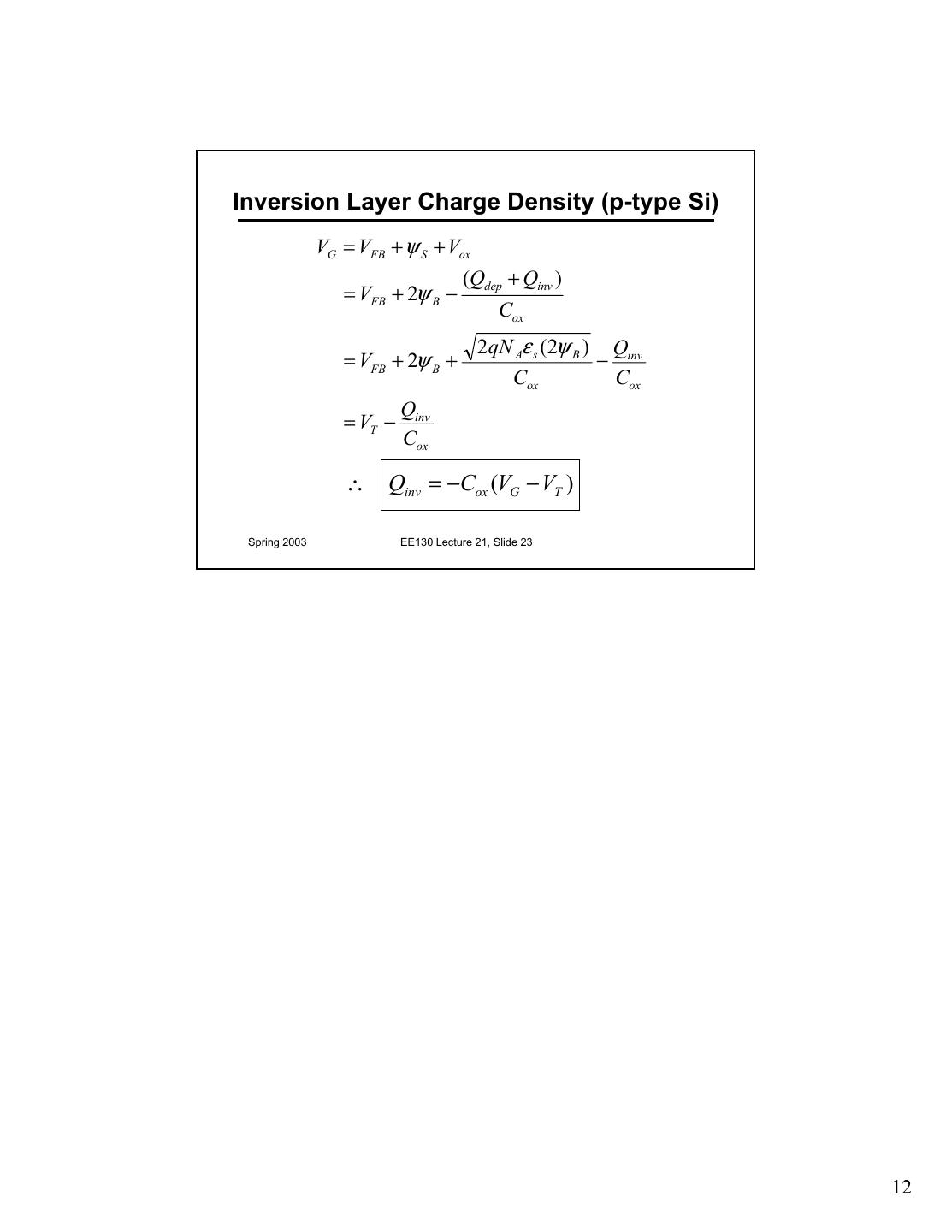
12 .Inversion Layer Charge Density (p-type Si) VG = VFB + ψ S + Vox (Qdep + Qinv ) = VFB + 2ψ B − Cox 2qN Aε s (2ψ B ) Qinv = VFB + 2ψ B + − Cox Cox Qinv = VT − Cox ∴ Qinv = −Cox (VG − VT ) Spring 2003 EE130 Lecture 21, Slide 23 12


