- 快召唤伙伴们来围观吧
- 微博 QQ QQ空间 贴吧
- 文档嵌入链接
- 复制
- 微信扫一扫分享
- 已成功复制到剪贴板
电荷耦合器件
展开查看详情
1 . Lecture #30 ANNOUNCEMENT • Review Session: Thu. May 15, 2-5 PM, 277 Cory OUTLINE • Charge coupled devices Spring 2003 EE130 Lecture 30, Slide 1 Memory Organization • Some address bits are used by row decoder to select one word line • Information in storage cells along that word line is passed to the column decoder • Decoder selects bits (according to the remaining address bits) to be presented at the output Spring 2003 EE130 Lecture 30, Slide 2 1
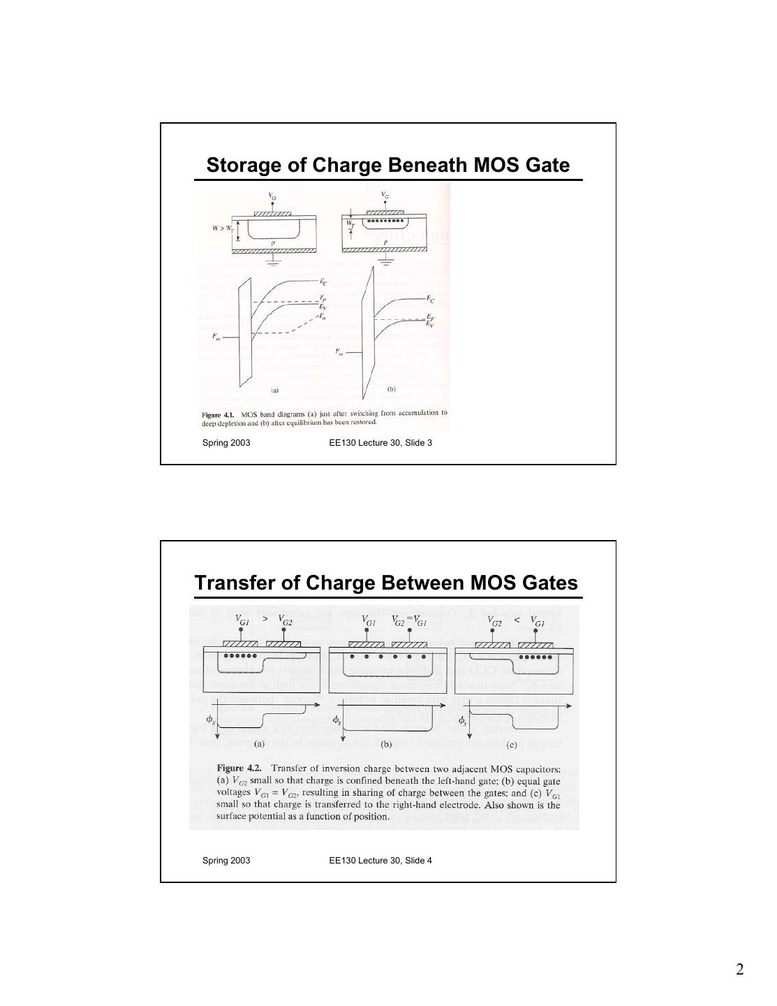
2 . Storage of Charge Beneath MOS Gate Spring 2003 EE130 Lecture 30, Slide 3 Transfer of Charge Between MOS Gates Spring 2003 EE130 Lecture 30, Slide 4 2
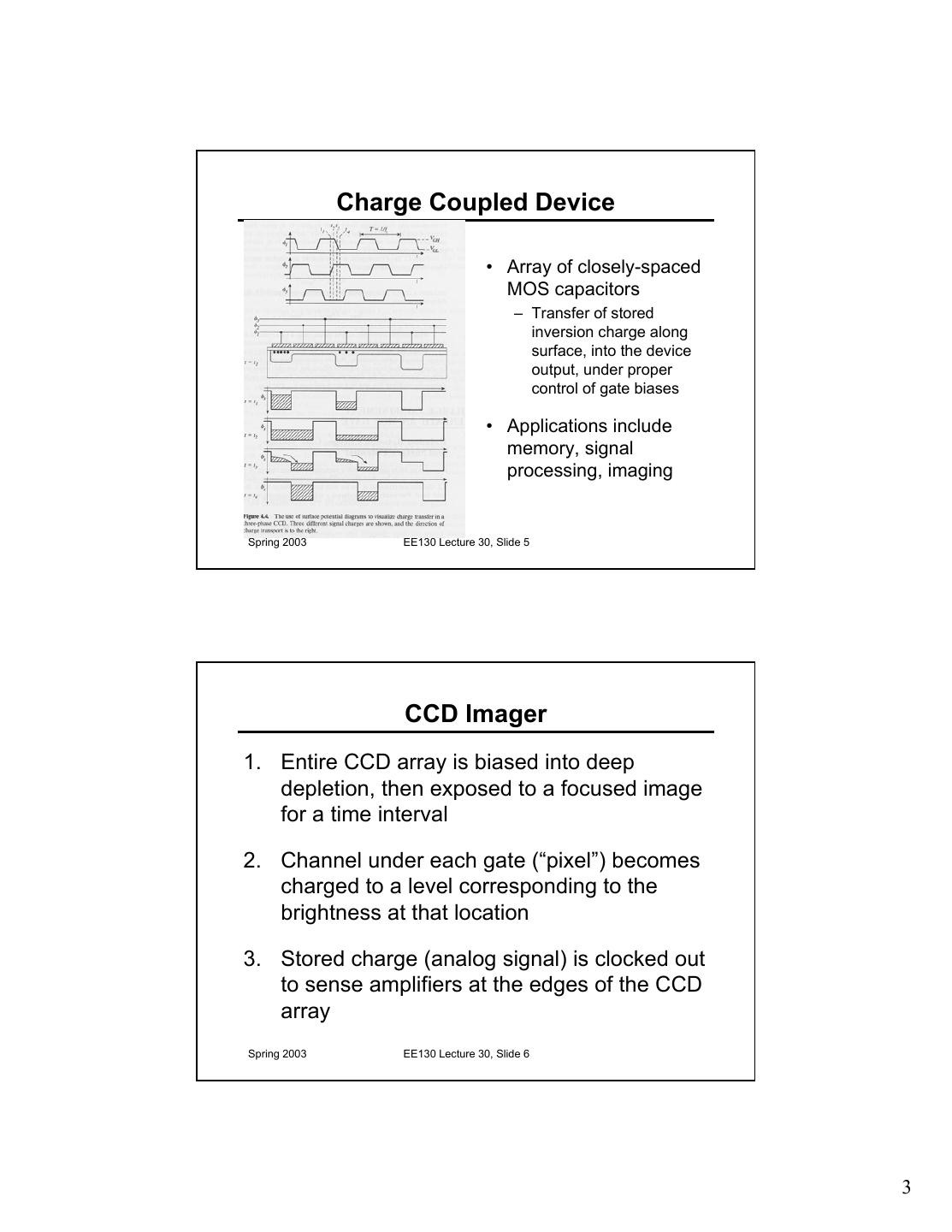
3 . Charge Coupled Device • Array of closely-spaced MOS capacitors – Transfer of stored inversion charge along surface, into the device output, under proper control of gate biases • Applications include memory, signal processing, imaging Spring 2003 EE130 Lecture 30, Slide 5 CCD Imager 1. Entire CCD array is biased into deep depletion, then exposed to a focused image for a time interval 2. Channel under each gate (“pixel”) becomes charged to a level corresponding to the brightness at that location 3. Stored charge (analog signal) is clocked out to sense amplifiers at the edges of the CCD array Spring 2003 EE130 Lecture 30, Slide 6 3


