- 快召唤伙伴们来围观吧
- 微博 QQ QQ空间 贴吧
- 文档嵌入链接
- 复制
- 微信扫一扫分享
- 已成功复制到剪贴板
双极结型晶体管
展开查看详情
1 .NJIT ECE271 Dr. Serhiy Levkov Chap 5 - 1 Topic 5 Bipolar Junction Transistors ECE 271 Electronic Circuits I
2 .NJIT ECE271 Dr. Serhiy Levkov Chapter Goals Explore physical structure of bipolar transistor Understand bipolar transistor action and importance of carrier transport across base region Study terminal characteristics of BJT. Explore differences between npn and pnp transistors. Define four operation regions of BJT. Explore simplified models for each operation region. Study Q-point Biasing of BJT. Chap 5 - 2
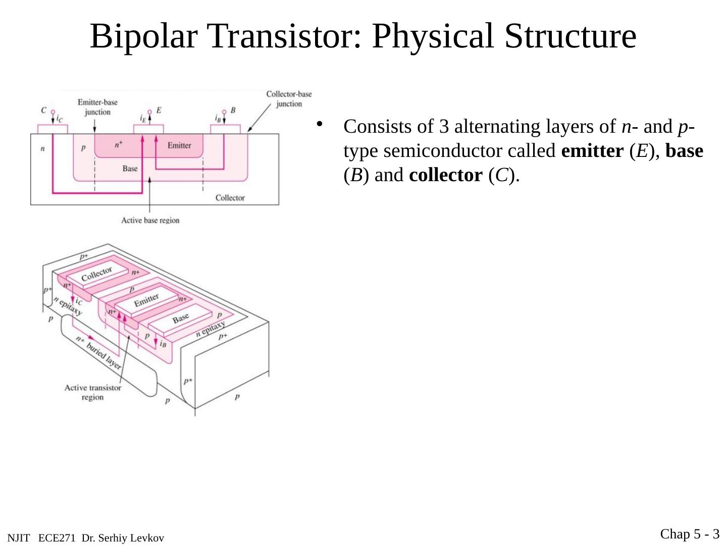
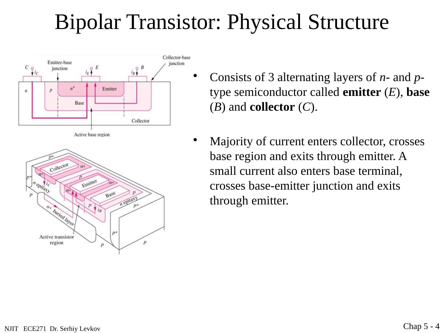
3 .NJIT ECE271 Dr. Serhiy Levkov Bipolar Transistor: Physical Structure Consists of 3 alternating layers of n - and p -type semiconductor called emitter ( E ), base ( B ) and collector ( C ). Chap 5 - 3
4 .NJIT ECE271 Dr. Serhiy Levkov Bipolar Transistor: Physical Structure Consists of 3 alternating layers of n - and p -type semiconductor called emitter ( E ), base ( B ) and collector ( C ). Majority of current enters collector, crosses base region and exits through emitter. A small current also enters base terminal, crosses base-emitter junction and exits through emitter . Chap 5 - 4
5 .NJIT ECE271 Dr. Serhiy Levkov Bipolar Transistor: Physical Structure Consists of 3 alternating layers of n - and p -type semiconductor called emitter ( E ), base ( B ) and collector ( C ). Majority of current enters collector, crosses base region and exits through emitter. A small current also enters base terminal, crosses base-emitter junction and exits through emitter. Carrier transport in the active base region directly beneath the heavily doped ( n + ) emitter dominates i -v characteristics of BJT. Chap 5 - 5
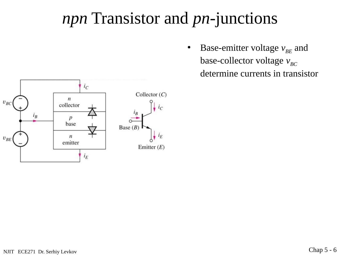
6 .NJIT ECE271 Dr. Serhiy Levkov npn Transistor and pn- junctions Base-emitter voltage v BE and base-collector voltage v BC determine currents in transistor Chap 5 - 6
7 .NJIT ECE271 Dr. Serhiy Levkov npn Transistor and pn- junctions Base-emitter voltage v BE and base-collector voltage v BC determine currents in transistor They are said to be positive when they forward-bias their respective pn junctions. Chap 5 - 7
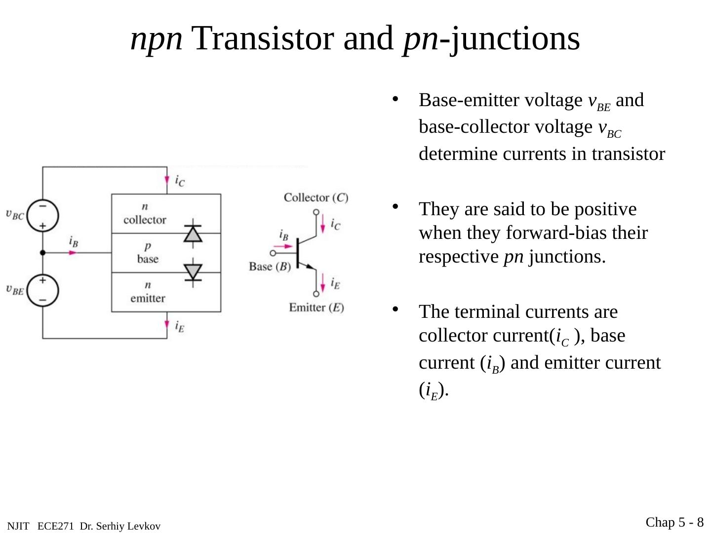
8 .NJIT ECE271 Dr. Serhiy Levkov npn Transistor and pn- junctions Base-emitter voltage v BE and base-collector voltage v BC determine currents in transistor They are said to be positive when they forward-bias their respective pn junctions. The terminal currents are collector current( i C ), base current ( i B ) and emitter current ( i E ). Chap 5 - 8
9 .NJIT ECE271 Dr. Serhiy Levkov npn Transistor and pn- junctions Base-emitter voltage v BE and base-collector voltage v BC determine currents in transistor They are said to be positive when they forward-bias their respective pn junctions. The terminal currents are collector current( i C ), base current ( i B ) and emitter current ( i E ). Primary difference between BJT and FET is that i B is significant while i G = 0. Chap 5 - 9
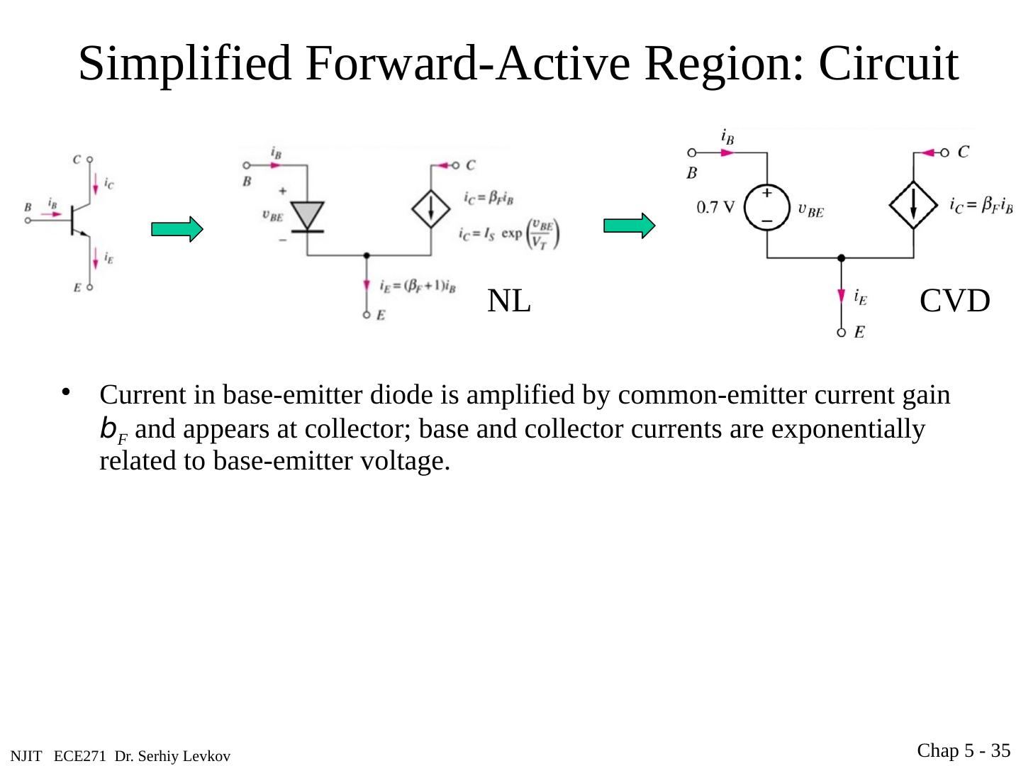
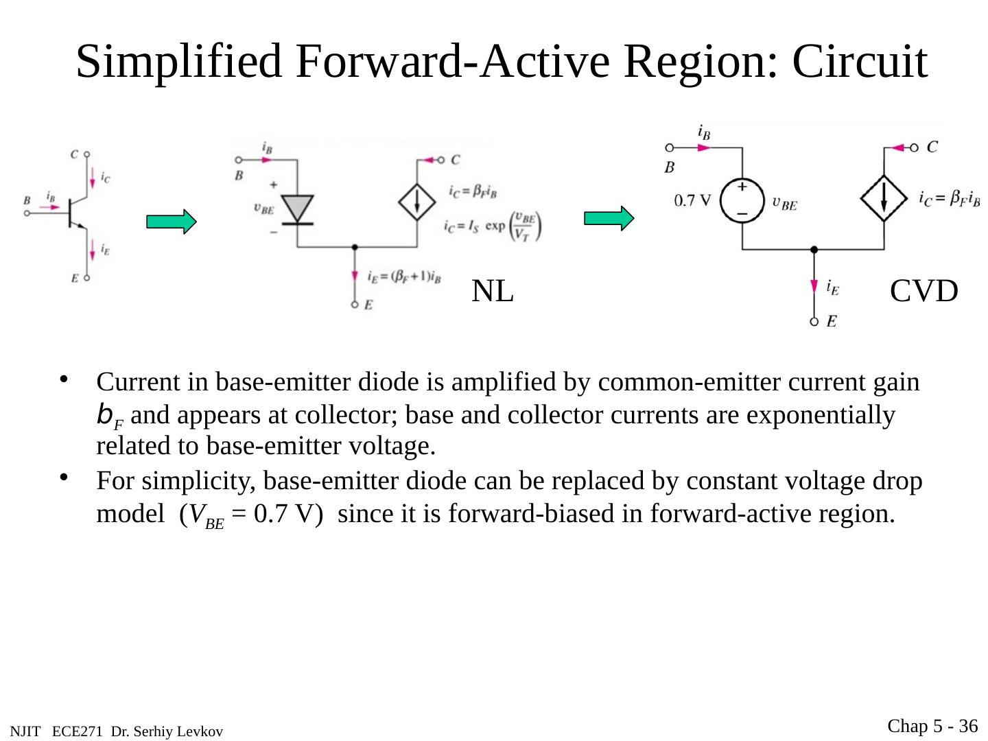
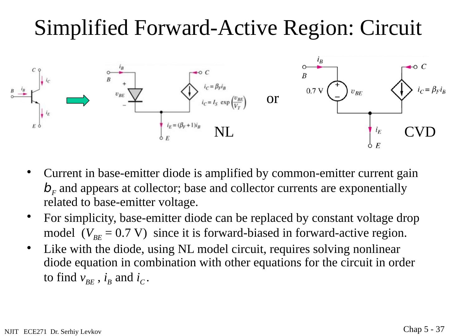
10 .NJIT ECE271 Dr. Serhiy Levkov npn Transistor: How it Works ( common emitter ) Left pn junction is forward biased – open. Right pn junction is reverse biased – closed. If those would be regular diodes – no current would exist btw emitter and collector. But the width of the base is very narrow, two back-to-back pn junctions are tightly coupled. Electrons injected from emitter into base region rush through it and are removed by collector, creating collector current I C . Some of the electrons will travel to the base, creating base current I B . Base current is usually quite smaller: where b is the common-emitter current gain usually is in the range 50 to 200. Thus transistor works as a current amplifier: Chap 5 - 10 Simulation: http://learnabout-electronics.org/bipolar_junction_transistors_05.php Look for relationship btw i B and i C .
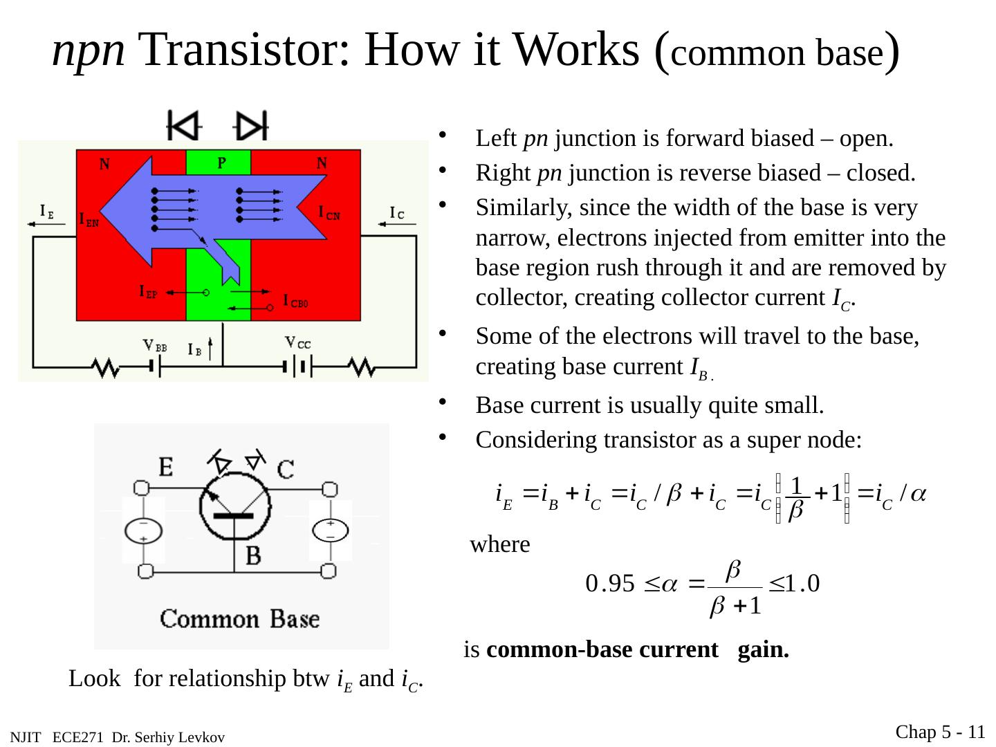
11 .NJIT ECE271 Dr. Serhiy Levkov npn Transistor: How it Works ( common base ) Left pn junction is forward biased – open. Right pn junction is reverse biased – closed. Similarly, since the width of the base is very narrow, electrons injected from emitter into the base region rush through it and are removed by collector, creating collector current I C . Some of the electrons will travel to the base, creating base current I B . Base current is usually quite small. Considering transistor as a super node: where is common-base current gain. Chap 5 - 11 Look for relationship btw i E and i C .
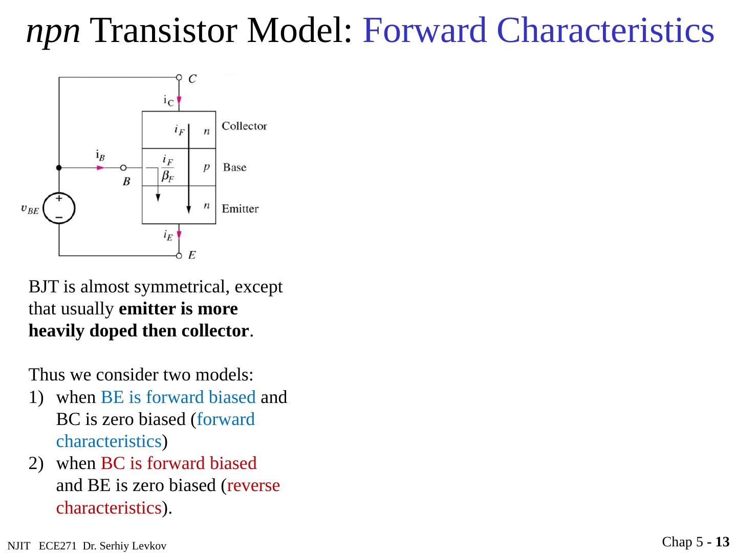
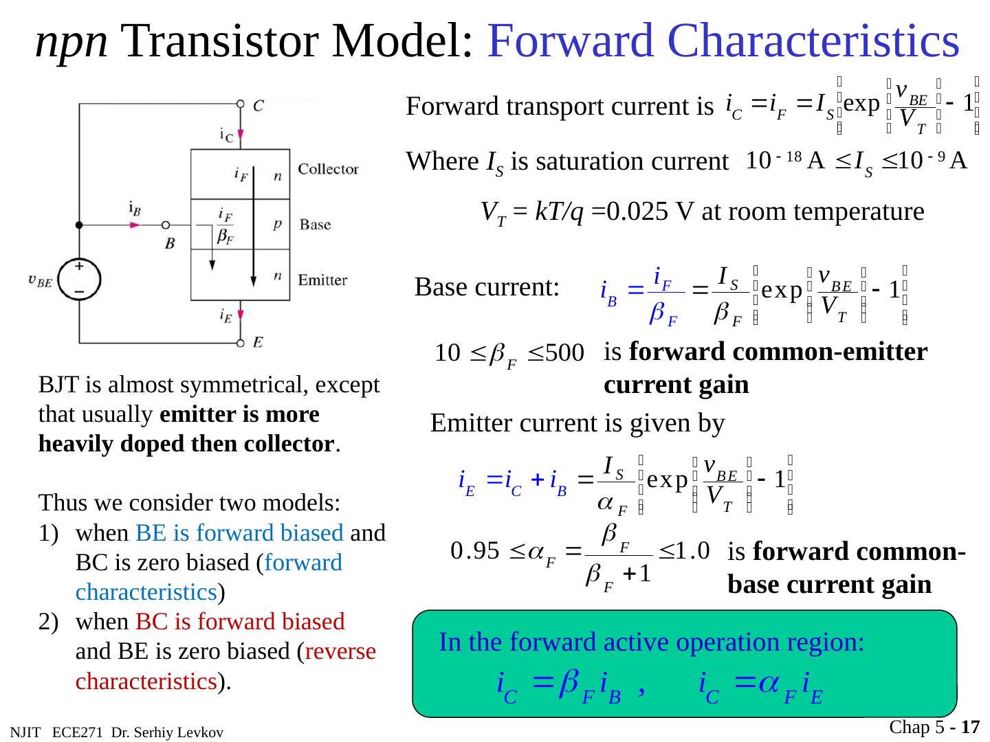
12 .NJIT ECE271 Dr. Serhiy Levkov npn Transistor Model: Forward Characteristics BJT is almost symmetrical, except that usually emitter is more heavily doped then collector . Thus we consider two models: when BE is forward biased and BC is zero biased ( forward characteristics ) Chap 5 - 12
13 .NJIT ECE271 Dr. Serhiy Levkov npn Transistor Model: Forward Characteristics BJT is almost symmetrical, except that usually emitter is more heavily doped then collector . Thus we consider two models: when BE is forward biased and BC is zero biased ( forward characteristics ) when BC is forward biased and BE is zero biased ( reverse characteristics ). Chap 5 - 13
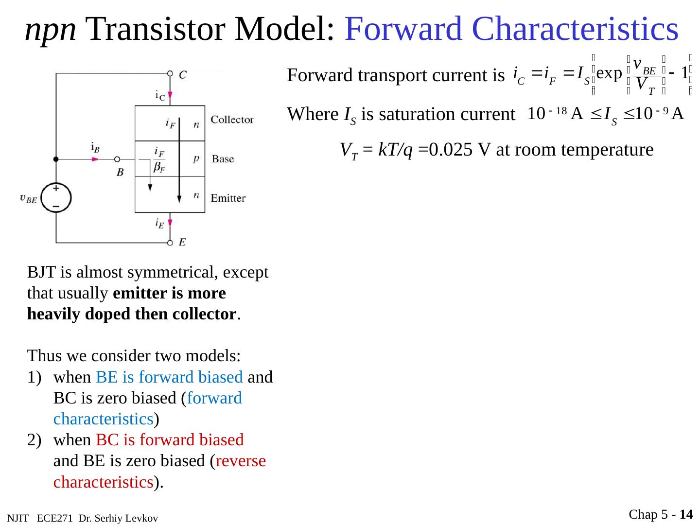
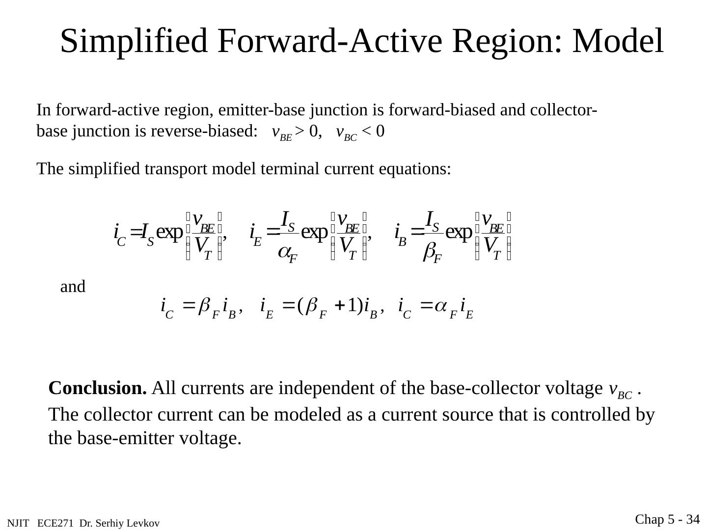
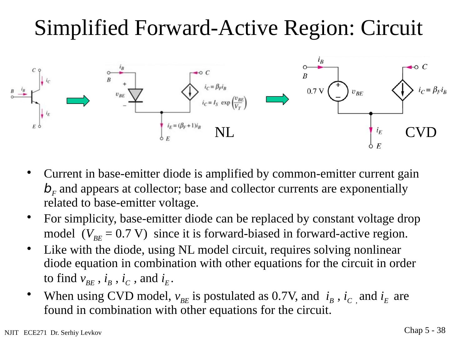
14 .NJIT ECE271 Dr. Serhiy Levkov npn Transistor Model: Forward Characteristics Forward transport current is Where I S is saturation current V T = kT/q =0.025 V at room temperature Chap 5 - 14 BJT is almost symmetrical, except that usually emitter is more heavily doped then collector . Thus we consider two models: when BE is forward biased and BC is zero biased ( forward characteristics ) when BC is forward biased and BE is zero biased ( reverse characteristics ).
15 .NJIT ECE271 Dr. Serhiy Levkov npn Transistor Model: Forward Characteristics Forward transport current is Where I S is saturation current V T = kT/q =0.025 V at room temperature is forward common-emitter current gain Chap 5 - 15 Base current: BJT is almost symmetrical, except that usually emitter is more heavily doped then collector . Thus we consider two models: when BE is forward biased and BC is zero biased ( forward characteristics ) when BC is forward biased and BE is zero biased ( reverse characteristics ).
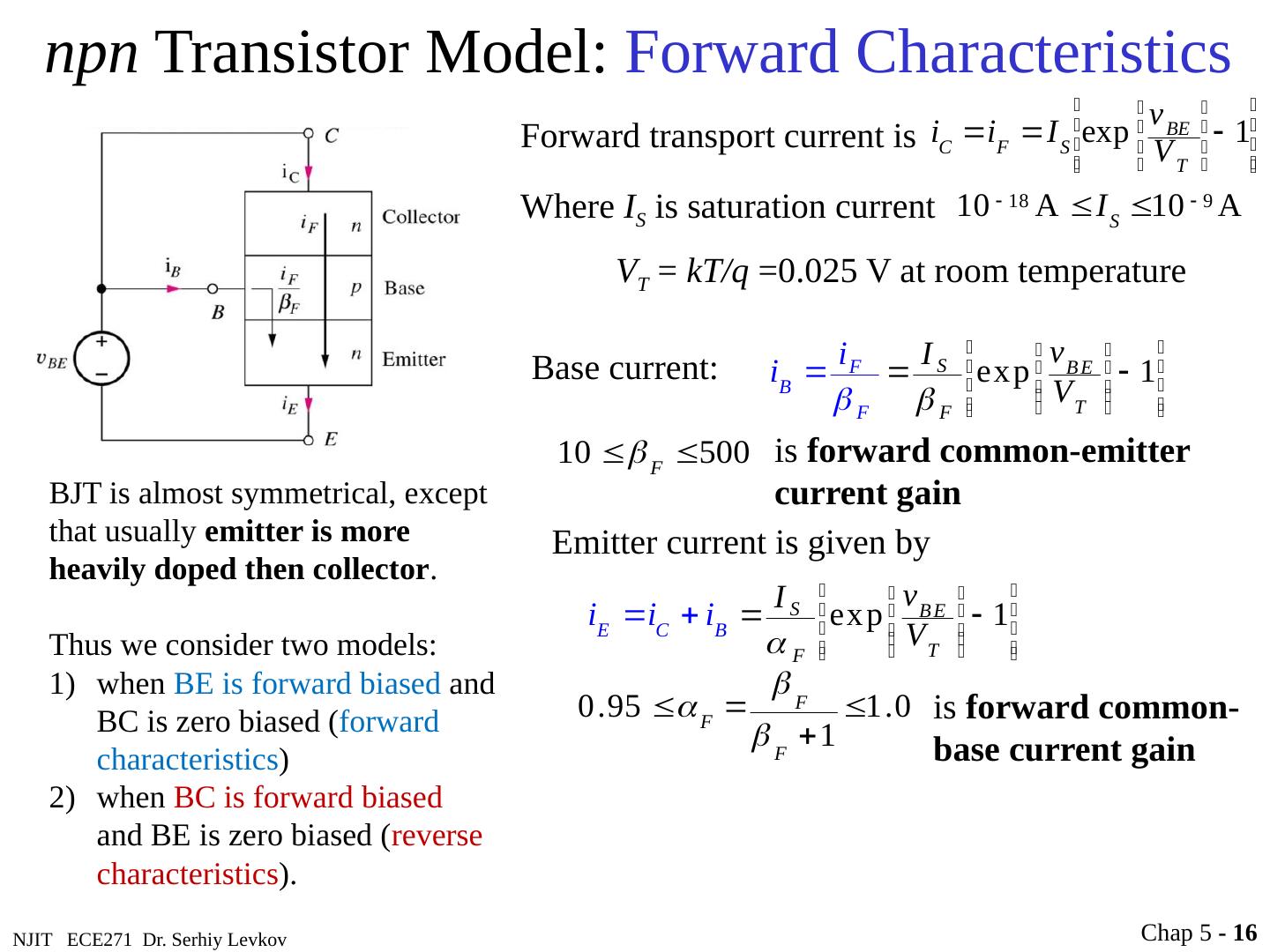
16 .NJIT ECE271 Dr. Serhiy Levkov npn Transistor Model: Forward Characteristics Forward transport current is Where I S is saturation current V T = kT/q =0.025 V at room temperature Emitter current is given by is forward common-emitter current gain is forward common- base current gain Chap 5 - 16 Base current: BJT is almost symmetrical, except that usually emitter is more heavily doped then collector . Thus we consider two models: when BE is forward biased and BC is zero biased ( forward characteristics ) when BC is forward biased and BE is zero biased ( reverse characteristics ).
17 .NJIT ECE271 Dr. Serhiy Levkov npn Transistor Model: Forward Characteristics Forward transport current is Where I S is saturation current V T = kT/q =0.025 V at room temperature Emitter current is given by is forward common-emitter current gain is forward common- base current gain In the forward active operation region: Chap 5 - 17 Base current: BJT is almost symmetrical, except that usually emitter is more heavily doped then collector . Thus we consider two models: when BE is forward biased and BC is zero biased ( forward characteristics ) when BC is forward biased and BE is zero biased ( reverse characteristics ).
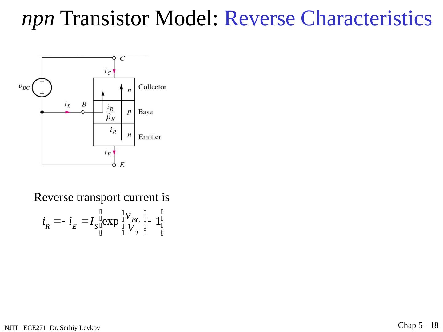
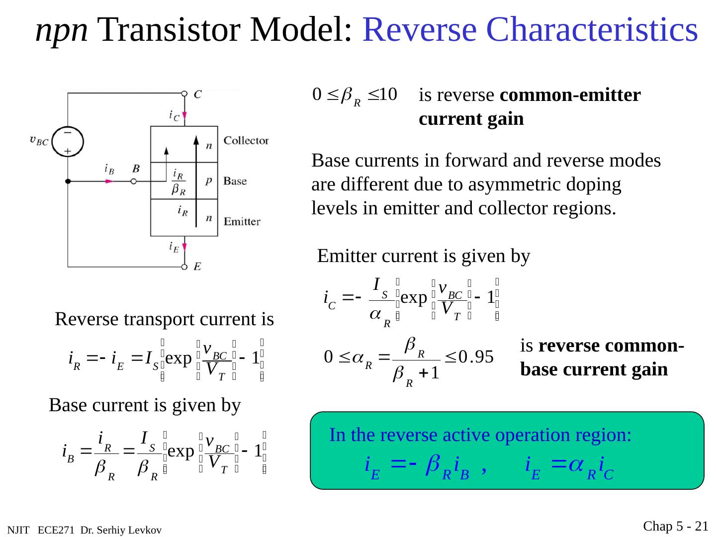
18 .NJIT ECE271 Dr. Serhiy Levkov npn Transistor Model: Reverse Characteristics Reverse transport current is Chap 5 - 18
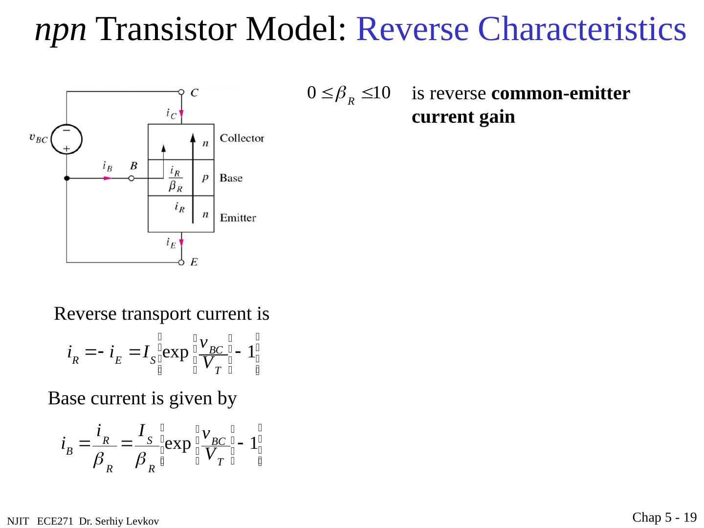
19 .NJIT ECE271 Dr. Serhiy Levkov npn Transistor Model: Reverse Characteristics Reverse transport current is Base current is given by Chap 5 - 19 is reverse common-emitter current gain
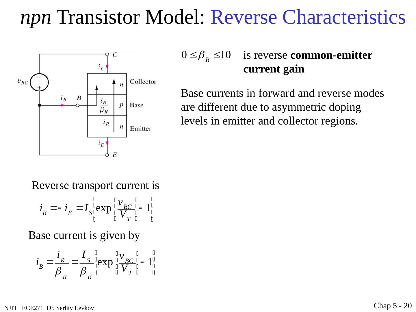
20 .NJIT ECE271 Dr. Serhiy Levkov npn Transistor Model: Reverse Characteristics Reverse transport current is is reverse common-emitter current gain Base current is given by Base currents in forward and reverse modes are different due to asymmetric doping levels in emitter and collector regions. Chap 5 - 20
21 .NJIT ECE271 Dr. Serhiy Levkov npn Transistor Model: Reverse Characteristics Reverse transport current is Emitter current is given by is reverse common-emitter current gain is reverse common-base current gain Base current is given by Base currents in forward and reverse modes are different due to asymmetric doping levels in emitter and collector regions. Chap 5 - 21 In the reverse active operation region:
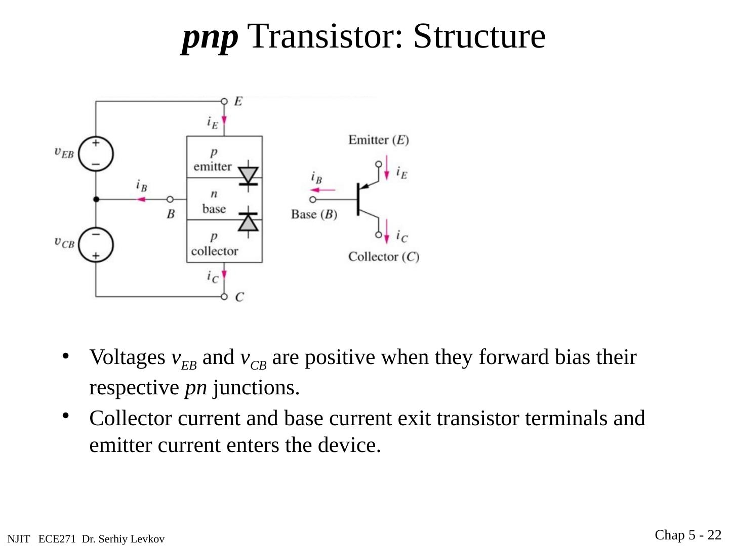
22 .NJIT ECE271 Dr. Serhiy Levkov pnp Transistor: Structure Voltages v EB and v CB are positive when they forward bias their respective pn junctions. Collector current and base current exit transistor terminals and emitter current enters the device. Chap 5 - 22
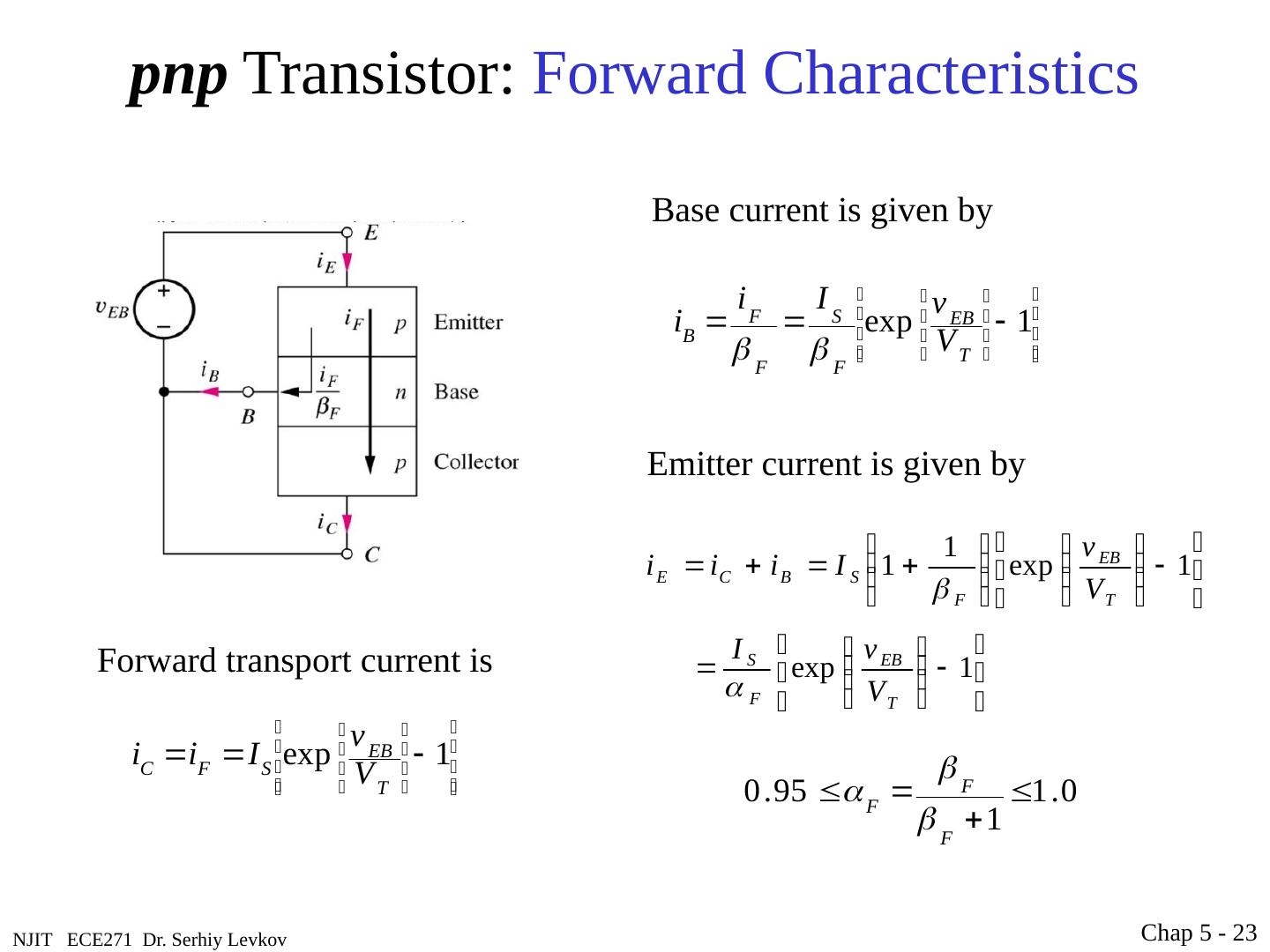
23 .NJIT ECE271 Dr. Serhiy Levkov pnp Transistor: Forward Characteristics Forward transport current is Base current is given by Emitter current is given by Chap 5 - 23
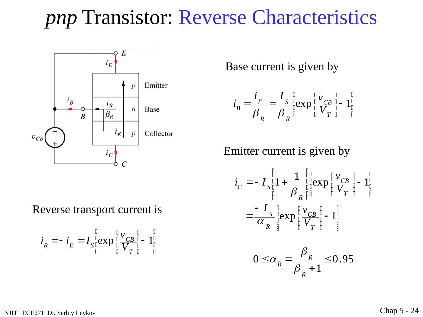
24 .NJIT ECE271 Dr. Serhiy Levkov pnp Transistor: Reverse Characteristics Reverse transport current is Base current is given by Emitter current is given by Chap 5 - 24
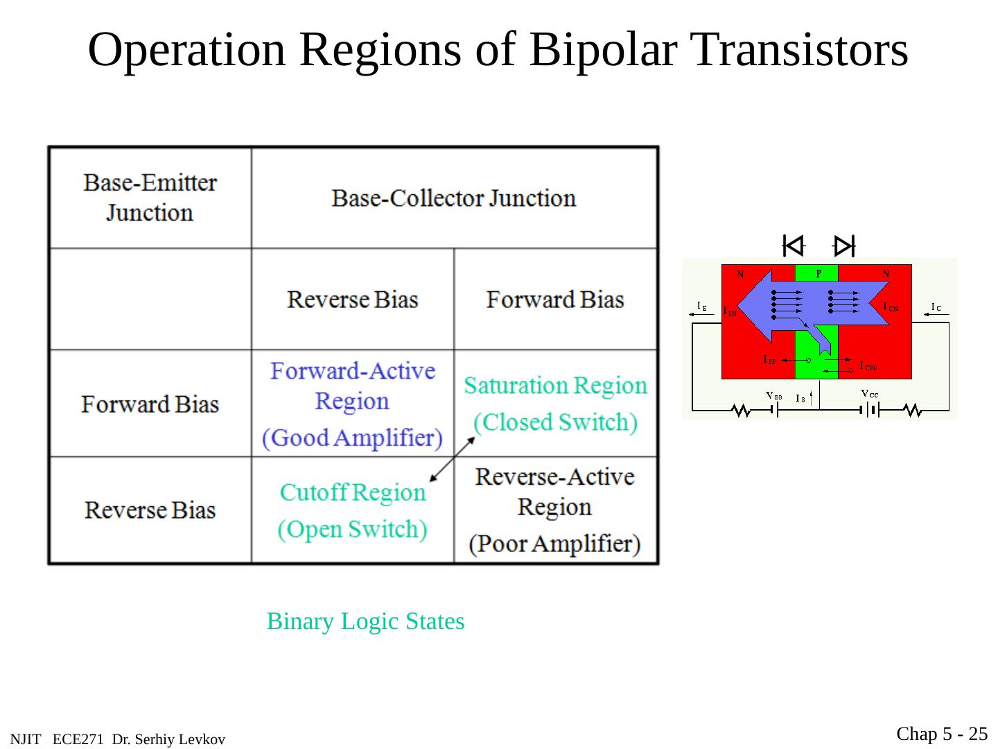
25 .NJIT ECE271 Dr. Serhiy Levkov Operation Regions of Bipolar Transistors Chap 5 - 25 Binary Logic States
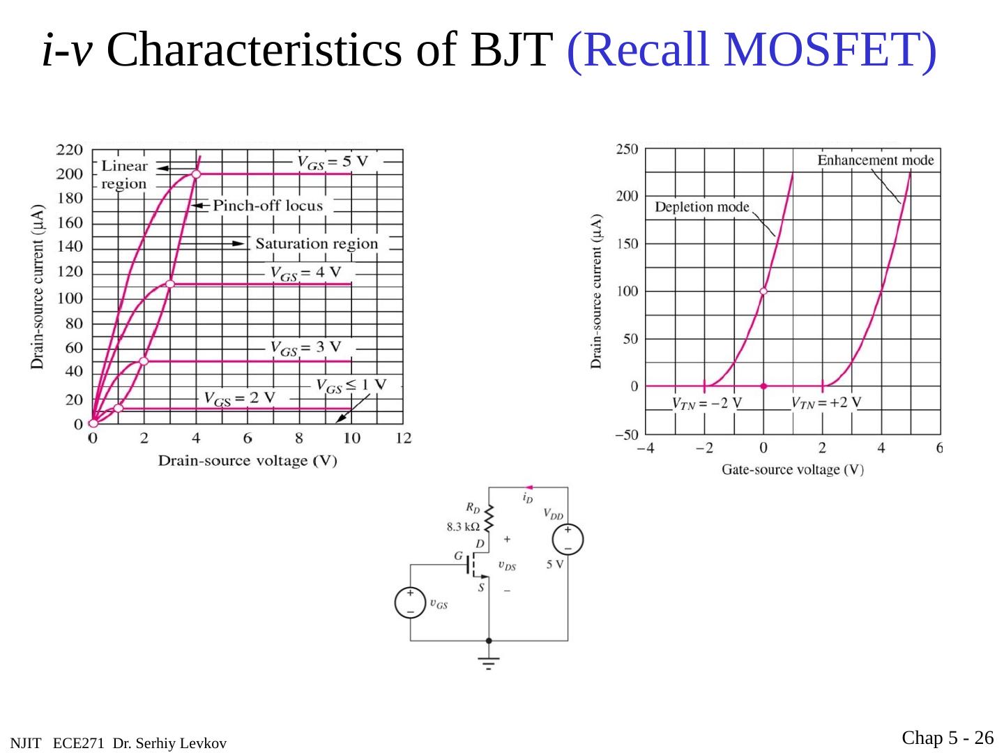
26 .NJIT ECE271 Dr. Serhiy Levkov i-v Characteristics of BJT (Recall MOSFET) Chap 5 - 26
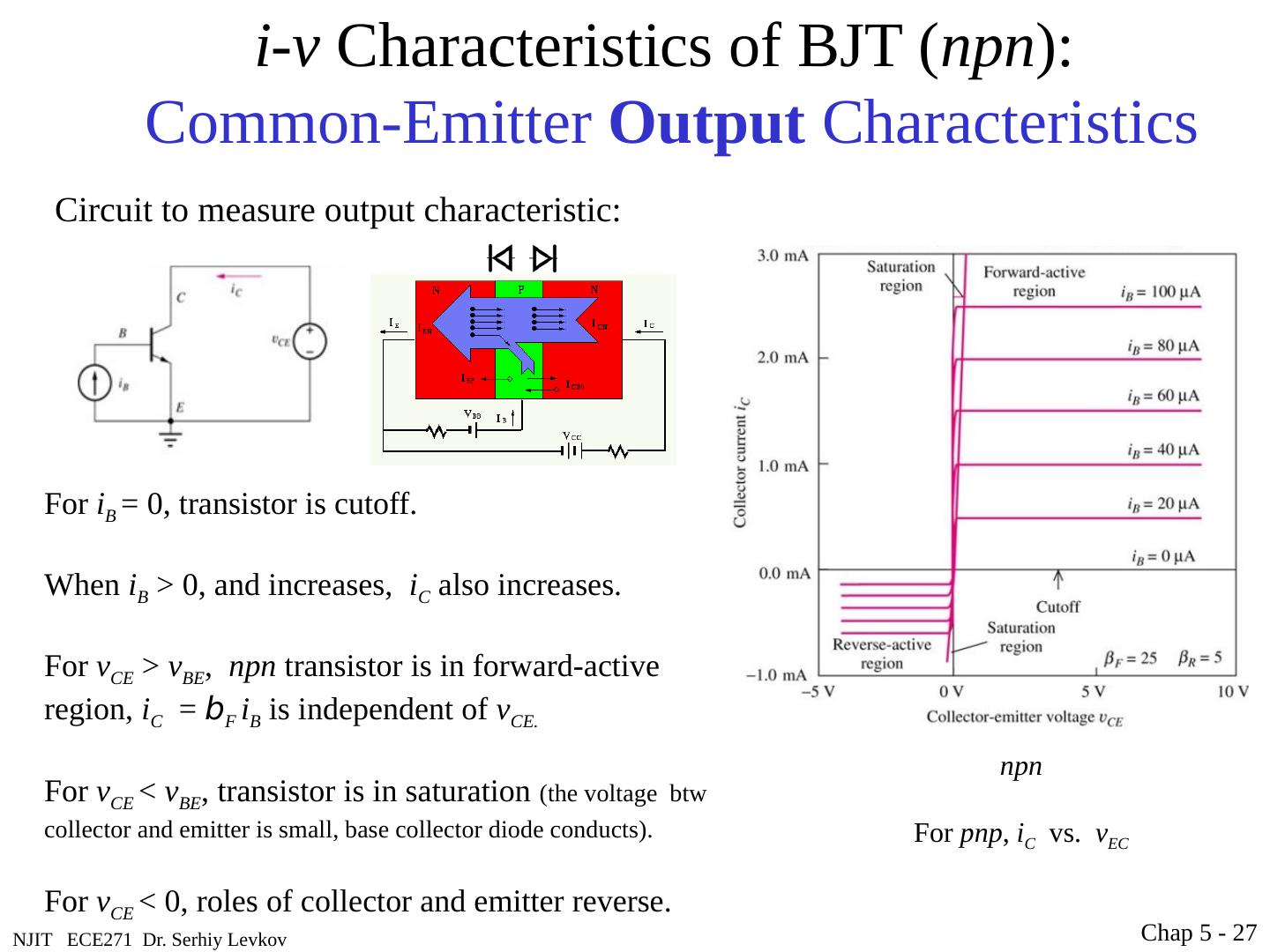
27 .NJIT ECE271 Dr. Serhiy Levkov i-v Characteristics of BJT ( npn ): Common-Emitter Output Characteristics For i B = 0, transistor is cutoff. When i B > 0, and increases, i C also increases. For v CE > v BE , npn transistor is in forward-active region, i C = b F i B is independent of v CE . For v CE < v BE , transistor is in saturation (the voltage btw collector and emitter is small, base collector diode conducts). For v CE < 0, roles of collector and emitter reverse. Chap 5 - 27 npn For pnp , i C vs. v EC Circuit to measure output characteristic:
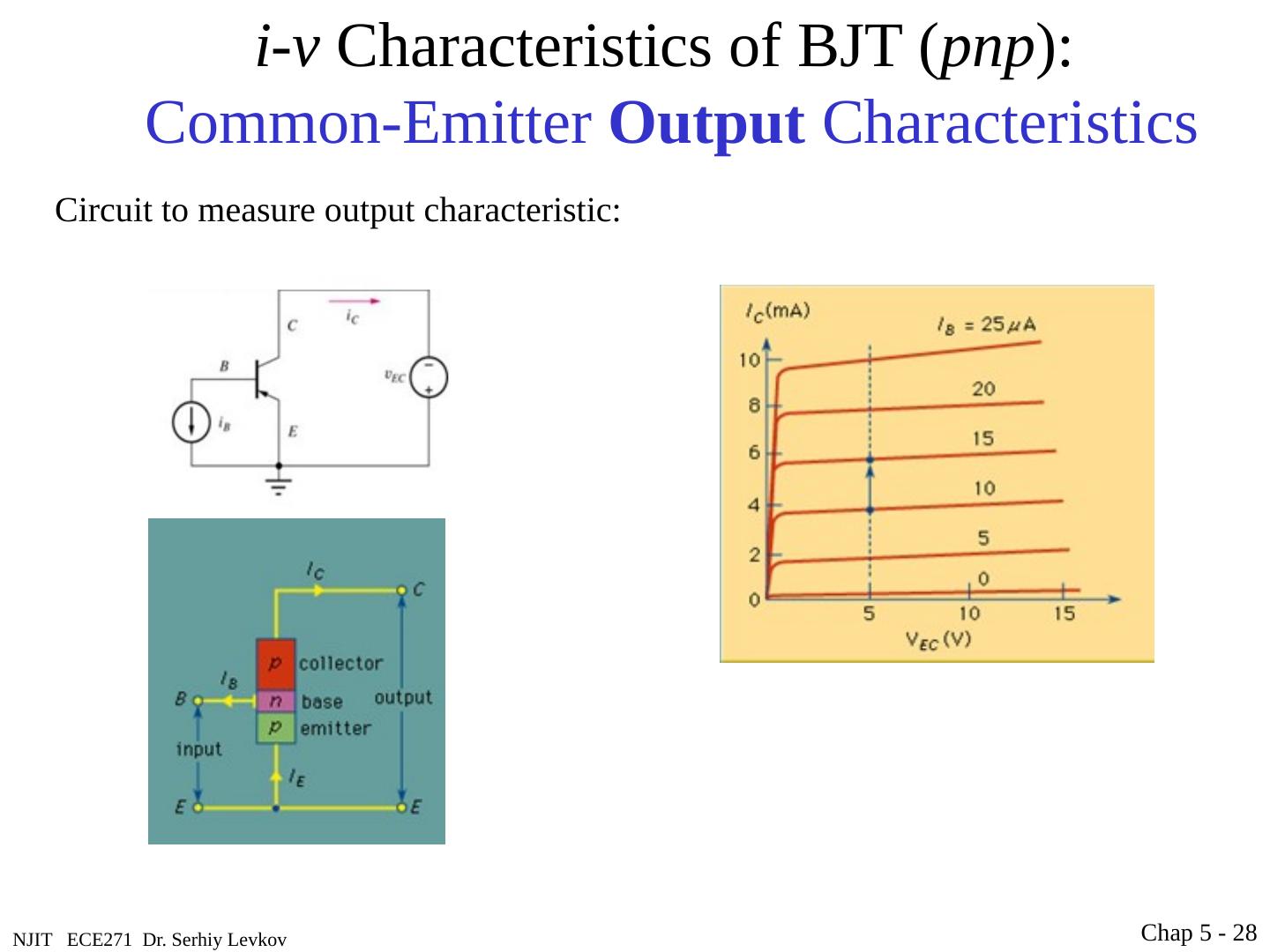
28 .NJIT ECE271 Dr. Serhiy Levkov Chap 5 - 28 Circuit to measure output characteristic: i-v Characteristics of BJT ( pnp ): Common-Emitter Output Characteristics
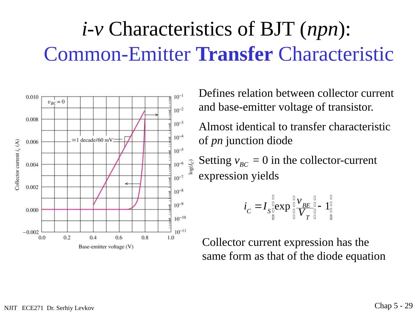
29 .NJIT ECE271 Dr. Serhiy Levkov i-v Characteristics of BJT ( npn ): Common-Emitter Transfer Characteristic Defines relation between collector current and base-emitter voltage of transistor. Almost identical to transfer characteristic of pn junction diode Setting v BC = 0 in the collector-current expression yields Chap 5 - 29 Collector current expression has the same form as that of the diode equation


