- 快召唤伙伴们来围观吧
- 微博 QQ QQ空间 贴吧
- 文档嵌入链接
- 复制
- 微信扫一扫分享
- 已成功复制到剪贴板
Analyzing 2TB of Raw Trace Data from a Manufacturing Process: A First Use Case
展开查看详情
1 .Analyzing 2TB of Raw Trace Data from a Manufacturing Process: A First Use Case of Apache Spark for Semiconductor Wafers from Real Industry Seungchul Lee, sclee@bistel.com BISTel Inc. Daeyoung Kim, dykim3@bistel.com BISTel Inc. #UnifiedAnalytics #SparkAISummit
2 .Contents • Introduction to BISTel – BISTel’s business and solutions – Big Data for BISTel’s smart manufacturing • Use cases of Apache Spark in manufacturing industry – Trace Analyzer (TA) – Map Analyzer (MA) #UnifiedAnalytics #SparkAISummit 2
3 .Introduction to BISTel #UnifiedAnalytics #SparkAISummit 3
4 .BISTel’s business areas • Providing analytic solutions based on Artificial Intelligence (AI) and Big Data to the customers for Smart Factory #UnifiedAnalytics #SparkAISummit 4
5 .BISTel’s solution areas • World-Class Manufacturing Intelligence through innovation #UnifiedAnalytics #SparkAISummit 5
6 .BISTel’s analytic solution: eDataLyzer #UnifiedAnalytics #SparkAISummit 6
7 .BISTel’s analytic solutions (MA) • Map Pattern Clustering – Automatically detect and classify map patterns with/without libraries – Process thousands of wafers and give results in few minutes Clustered Defective wafers #UnifiedAnalytics #SparkAISummit 7
8 .BISTel’s analytic solutions (TA) • Specialized Application for Trace Raw Data – Extracts the vital signs out of equipment trace data – Provide in-depth analysis which traditional methods cannot reach Normal Abnormal #UnifiedAnalytics #SparkAISummit 8
9 .BISTel’s big data experiences #UnifiedAnalytics #SparkAISummit 9
10 .BISTel’s big data experiences - YMA Test using Spark - - Big data platforms comparison- #UnifiedAnalytics #SparkAISummit 10
11 .Trace Analyzer (TA) #UnifiedAnalytics #SparkAISummit 11
12 .Trace Data • Trace Data is sensor data collected from processing equipment within a semiconductor fab during a process run. - Wafer - - Semiconductor industry - #UnifiedAnalytics #SparkAISummit 12
13 . Logical Hierarchy of the trace data wafer Wafer Lot Visualization Whole process Recipe Step Recipe Process Recipe 1 Process #UnifiedAnalytics #SparkAISummit 13
14 . An example of the trace data Process Recipe Recipe step Lot Wafer Param1 Param2 Time 2015-01-20 021_LIT RecipeA 1 1501001 1 32.5 45.4 09:00:00 #UnifiedAnalytics #SparkAISummit 14
15 .Data attributes • Base unit : one process and one parameters • 1000 wafers • Each wafer has 1000~2000 data points in a recipe step • Some factors that make trace data huge volume • # of parameters • # of processes • # of wafers • # of recipe steps • duration of the recipe step #UnifiedAnalytics #SparkAISummit 15
16 .An example of the trace data – (2) Parameter # of # of Avg. Recipe Data # of No. Fab per unit processes recipe steps Process Time Frequency units (max) 1 Array 109 10 16 mins 1Hz 288 185 2 CF 25 5 1min 1Hz 154 340 3 CELL 12 7 1min 1Hz 213 326 4 MDL 5 12 2mins 1Hz 32 154 • Some calculations • For one process, one parameter and one wafer • 16 * 10 * 60 sec * 1Hz = 9600 points • Multi parameters, multi processes and multi wafers • 9600 * 288 *185 * 109 * (# of wafers) #UnifiedAnalytics #SparkAISummit 16
17 .Spark : Smart manufacturing • Spark is a best way to process big data in batch analytics • Distributing data based on parameter is suitable for using Apache Spark. • Easy deployment and scalability when it comes to providing the solutions to our customers #UnifiedAnalytics #SparkAISummit 17
18 .Naïve way: applying spark to TA #UnifiedAnalytics #SparkAISummit 18
19 .How to apply Spark to TA? traceDataSet = config.getTraceRDDs().mapToPair(t->{ String recipeStepKey = TAUtil.getRecipeStepKey(t); #use recipe step as key return new Tuple2<String,String>(recipeStepKey,t); }).groupByKey(); traceDataSet.flatMap(t->{ Map<String,TraceDataSet> alltraceData = TAUtil.getTraceDataSet(t); ... TAUtil.seperateFocusNonFocus(alltraceData,focus,nonFocus); #separate data ta.runTraceAnalytic(focus,nonFocus,config); # calling the TA core ... });
20 .Most cases in manufacturing industry • In real industry, most parameters have small number of data points. (Most case : 1Hz) • In addition, the number of wafers to be analyzed is not massive. (up to 1,000 wafers) • Therefore the total number of data points in a process can be easily processed in a core
21 .Issues in manufacturing industry • Last year, I have got an email indicating that.. #UnifiedAnalytics #SparkAISummit 21
22 .Big parameter • Tools with high frequency or high recipe time can produce huge volume for single parameter • Requirements in industry • For one parameter • 400,000 wafers • 20,000 data points. #UnifiedAnalytics #SparkAISummit 22
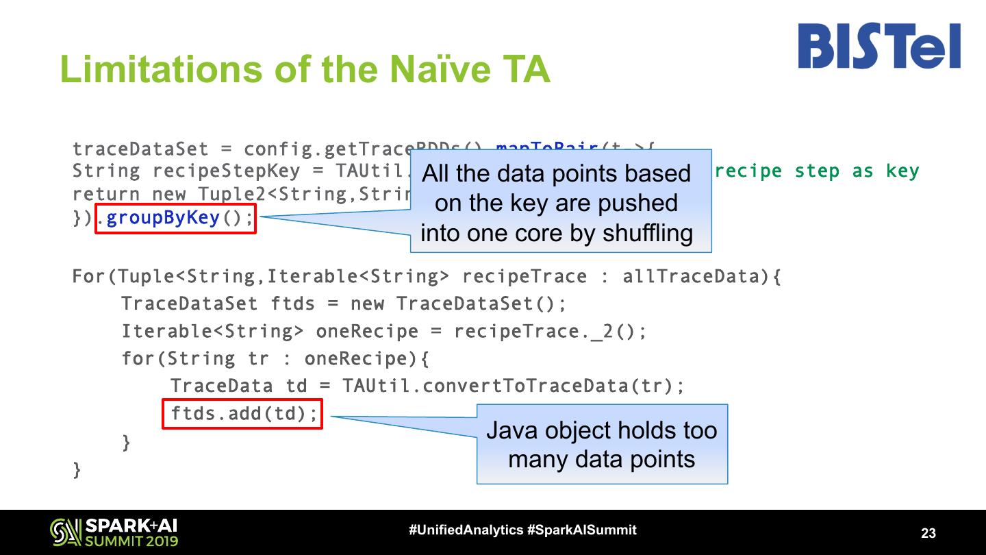
23 .Limitations of the Naïve TA traceDataSet = config.getTraceRDDs().mapToPair(t->{ String recipeStepKey = TAUtil.getRecipeStepKey(t); #use recipe step as key All the data points based return new Tuple2<String,String>(recipeStepKey,t); }).groupByKey(); on the key are pushed into one core by shuffling For(Tuple<String,Iterable<String> recipeTrace : allTraceData){ TraceDataSet ftds = new TraceDataSet(); Iterable<String> oneRecipe = recipeTrace._2(); for(String tr : oneRecipe){ TraceData td = TAUtil.convertToTraceData(tr); ftds.add(td); } Java object holds too } many data points #UnifiedAnalytics #SparkAISummit 23
24 .Needs for new TA spark • Naïve TA Spark version cannot process massive data points. • Nowadays, new technology enhancements enable data capture at much higher frequencies. • TA for “big parameter” version is necessary. #UnifiedAnalytics #SparkAISummit 24
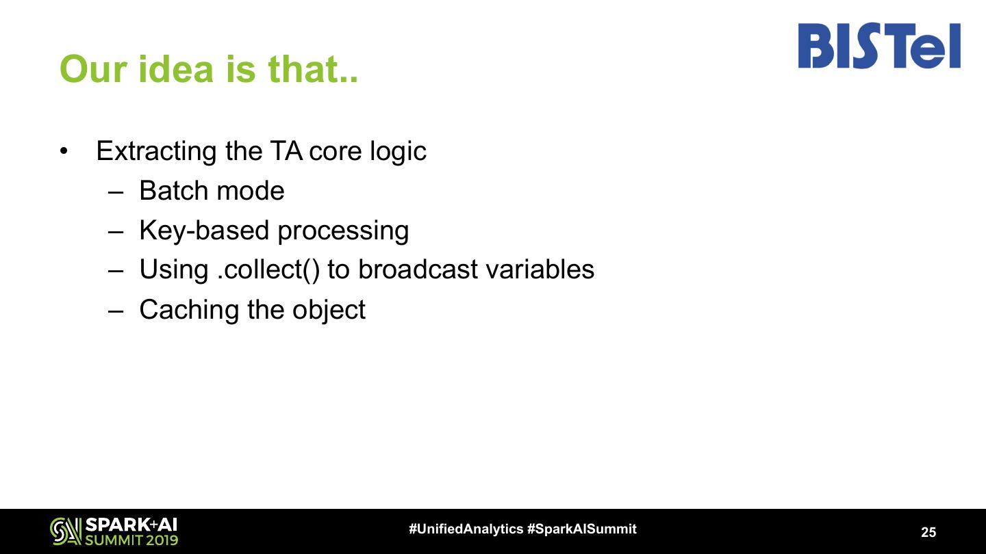
25 .Our idea is that.. • Extracting the TA core logic – Batch mode – Key-based processing – Using .collect() to broadcast variables – Caching the object #UnifiedAnalytics #SparkAISummit 25
26 .Batch First element : process, recipe step, parameter and batch ID • Preprocessing trace data Second element : lot, wafer and trace values JavaPairRDD<String, List<String>> traceDataRDD = TAImpl.generateBatch(traceData) • Key-based processing Summary • Base unit : process key or recipe step key statistics . . . •Param A #UnifiedAnalytics #SparkAISummit 26
27 .Collect() : TA Cleaner • Filtering out traces that have unusual duration of process time. • Use the three main Spark APIs – mapToPair : extract relevant information – reduceByKey : aggregating values based on the key – collect : send the data to the driver #UnifiedAnalytics #SparkAISummit 27
28 .Collect() : TA Cleaner – (2) • traceData.mapToPair() • Return • key : process • value : wafer and its length Worker Worker Worker Worker wafer value wafer value wafer value wafer value 1 65 1 83 1 34 1 71 2 54 2 54 2 77 2 80 … … … … … … … … #UnifiedAnalytics #SparkAISummit 28
29 .Collect() : TA Cleaner – (3) • reduceByKey() • Aggregating contexts into one based on the process key wafer value wafer value 1 65 1 88 2 54 2 92 … … … … wafer value Shuffling 1 153 2 146 … … #UnifiedAnalytics #SparkAISummit 29

